SNLA246C October 2015 – April 2024 DP83867CR , DP83867CS , DP83867E , DP83867IR , DP83867IS
- 1
- Trademarks
- 1Introduction
- 2Troubleshooting the Application
-
3Application Specific
Debugs
- 3.1 Improving Link-up Margins for Short Cables
- 3.2 Improving Link Margins across Different Channels
- 3.3 Link up in 100Mbps Full Duplex Force Mode
- 3.4 Unstable Link Up Debug in 1Gbps communication
- 3.5 DP83867PHY and DP83867PHY Cannot Link Up in 1Gbps
- 3.6 Compliance Debug
- 3.7 EMC Debug
- 3.8 Tools and References
- 4Conclusion
- 5References
- 6Revision History
1 Introduction
The DP83867 is a robust, low power, fully featured Physical Layer transceiver with integrated PMD sublayers to support the 10BASE-Te, 100BASE-TX, and 1000BASE-T Ethernet protocols.
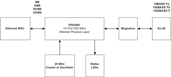
Figure 1-1 is a high-level system block diagram of a typical DP83867 application.
 Figure 1-1 DP83867 Block Diagram
The DP83867 can connect to an Ethernet MAC and to a media. The connection to the media is via a transformer and a connector.
Table 1-1 DP83867 Configurations
| DP83867 Version | MAC interface | Pin number/ package |
|---|---|---|
| DP83867IR/CR | RGMII | 48 pins / QFN package |
| DP83867IS/CS/DP83867E | SGMII | 48 pins/ QFNpackage |
| DP83867IRPAPR | MII/GMII/RGMII | 64 pins / QFP package |
Note: This Debug application note mainly focuses on
RGMII and SGMII interface debug