SNLA246C October 2015 – April 2024 DP83867CR , DP83867CS , DP83867E , DP83867IR , DP83867IS
- 1
- Trademarks
- 1Introduction
- 2Troubleshooting the Application
-
3Application Specific
Debugs
- 3.1 Improving Link-up Margins for Short Cables
- 3.2 Improving Link Margins across Different Channels
- 3.3 Link up in 100Mbps Full Duplex Force Mode
- 3.4 Unstable Link Up Debug in 1Gbps communication
- 3.5 DP83867PHY and DP83867PHY Cannot Link Up in 1Gbps
- 3.6 Compliance Debug
- 3.7 EMC Debug
- 3.8 Tools and References
- 4Conclusion
- 5References
- 6Revision History
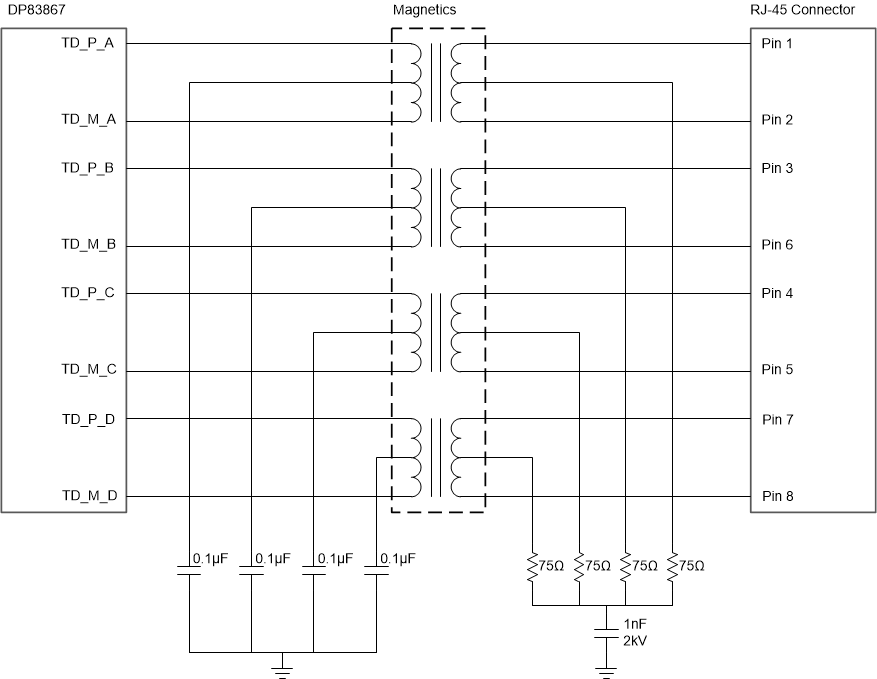
3.6 Compliance Debug
The following section mainly go over the general guideline on how to debug compliance issue on DP83867PHY.
- Check the schematic
- Make sure the Transformer follow data sheet specification in Section 2.3.1.
- No shorted center taps on transformer
- Double check on the capacitors on the center taps of transformer
- Remove ESD diodes on MDI lines for compliance test
- Check Rbias value and make sure the value falls in the 1% range
- Follow the schematic check list recommendation in Section 2.2
- Check the layout
- Make sure no clock signal and data signal near the MDI lines
- Check length matching and impedance matching (100ohms) for MDI lines
- No vias around the MDI lines
- Follow the layout checklist in Section 2.2
- Check the compliance test How to Configure DP8386x for Ethernet Compliance Testing application note. Follow the procedure on the compliance test application note.
- If all schematic, layout
checklist, and compliance test application note do not help, adjusting register
0x00A0, 0x00A1, 0x00A2, 0x00A3 can help with compliance test.Note: Default values of 0x00A1 and 0x00A2 registers are trimmed.