SNLA434 November 2023 DP83TC812R-Q1 , DP83TD510E , DP83TG720R-Q1 , LMK1C1103 , LMK1C1104 , LMK5B12204 , LMK6C
2.4.1 Topology 1
Using a crystal to clock the IC’s, it is important to read the crystal data sheet and the IC’s data sheet to confirm that the two parts are able to work together. With that being done, a typical crystal connection can look like the following.
R2 and R3 is the series termination of the crystal and R1 is the parallel termination of the crystal, these resistors can be added to the circuit but can also be removed to achieve smaller traces. However, the use of those resistors can be mandated from the IC data sheet.
The C1 and C2 capacitors are important to use C0G/NP0 capacitors for proper performance on system level.
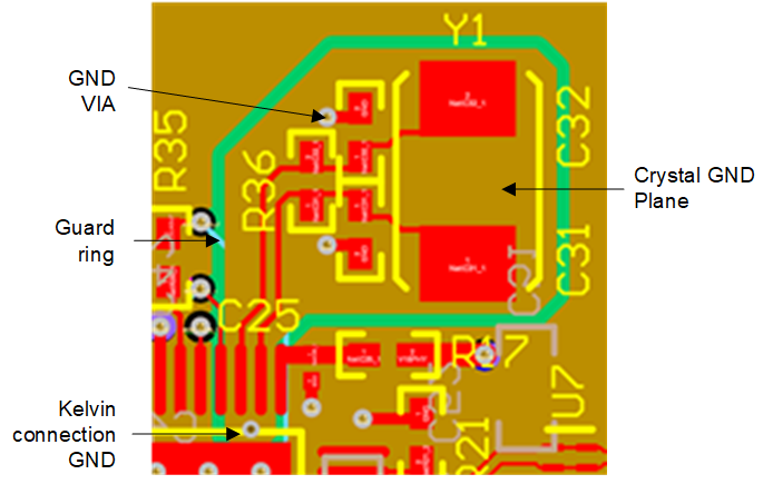
 Figure 2-13 Clock
Layout -
 Option 1 |
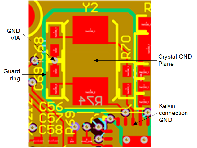
 Figure 2-14 Clock
Layout - Option 2
 |
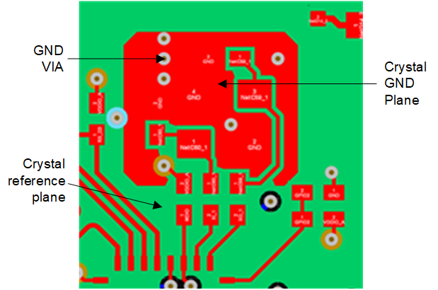
 Figure 2-15 Clock
Layout - Option 3
 |
As shown in the layout examples, the suggestion is to have the crystal ground connected on an island, keeping noise away from the system ground. However there is an importance to keep this crystal ground kelvin connected to the system ground to make sure this island ground is not susceptible to high-frequency ringing.