SNOA475F October 2016 – September 2020 LMV791
- Trademarks
- 1Introduction
-
2What Parameters Should Be Tested?
- 2.1 Open-Loop Gain (AOL) and Phase Margin
- 2.2 Slew Rate
- 2.3 Common-Mode Rejection Ratio (CMRR) and Power Supply Rejection Ratio (PSRR)
- 2.4 Open-Loop Output Impedance (Zo)
- 2.5 Voltage Noise (en)
- 2.6 Current Noise (in)
- 2.7 Input Offset Voltage (VOS), Input Bias Current (Ib), and Quiescent Current (IQ)
- 2.8 Output Voltage Versus Output Current (Claw Curve)
- 2.9 Overload Recovery Time (tOR)
- 2.10 Common-mode Input Capacitance (CCM) and Common-mode Differential Capacitance (CDIFF)
- 2.11 Overshoot and Transient Response
- 2.12 Common-Mode Voltage Range (CMVR)
- 3Conclusion
- Revision History
2.3 Common-Mode Rejection Ratio (CMRR) and Power Supply Rejection Ratio (PSRR)
Common-Mode Rejection Ratio (CMRR) and Power Supply Rejection Ratio (PSRR) are two parameters not always modeled but they can be equally important. Common mode voltage is defined as the average voltage at both inverting and non-inverting input of an op amp.

CMRR quantifies how well an op amp rejects common mode signals, such as common mode noise. Hence, higher value is better because more of the common mode signal is rejected and therefore has less effect on the op amp. Common mode effect on output can be shown as follows:

CMRR changes across frequency. CMRR is highest at lower frequencies, usually in the range of 80 dB to 160 dB at DC. CMRR rolls off at higher frequencies, so when selecting a device make sure CMRR performance is sufficient at higher frequcies of interest. CMRR is especially important in non-inverting configurations because the common-mode voltage is equal to the input voltage. CMRR is defined as the ratio of op amp's open-loop differential gain (ADM) to its open-loop common mode gain (ACM). In reality, these two gain characteristics can be tricky to isolate from one another. Luckily, the power of simulation allows the user to do it effectively. For more information on CMRR please refer to Texas Instruments Precision Labs video series on CMRR.

Figure 2-7 below shows "CMRR Test Circuit". This test circuit uses two copies of an op amp under test to measure the ADM and ACM separately. In the top circuit, AC source VIN is applied to both input of op amp to create a clean common mode input signal. Inductor L1 acts as a short at DC and an open circuit at AC to allow for both a valid DC operating point and measurement of the ACM.
In the bottom circuit, AC source VIN is routed to voltage controlled voltage sources E1 and E2. This generates a differential version of VIN biased around 0V, which is then applied to the input of the op amp. Similar to the top circuit, inductor L2 acts as a short circuit at DC and open circuit at AC to allow for both a valid DC operating point and measurement of ADM.
It is important to check the DC operating point to ensure that the op amp is operating in its linear region. Make sure to match the specified data sheet conditions such as: power-supply voltage common mode voltage, capacitive and resistive loads (CL and RL). To measure CMRR, run an AC transfer characteristics over the desired frequency range and plot the magnitude in dB for ACM and ADM. Then use the post-processing tool to generate the curve for ADM over ACM (the definition of CMRR). Figure 2-10 shows the simulated CMRR result for TLV9102. For a more complete simulation test analysis, please refer to the following EDN article, authored by Ian Williams. This circuit may be simulated by downloading the AN1516 Test Circuits in either TINA-TI™ or PSpice® for TI.
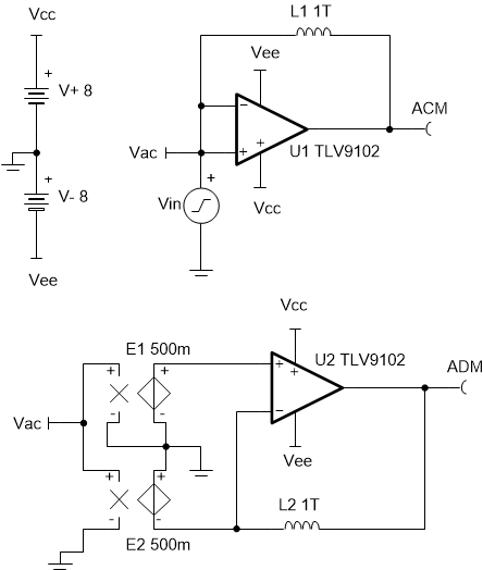 Figure 2-7 Common-Mode Rejection Ratio
(CMRR) Test Circuit
Figure 2-7 Common-Mode Rejection Ratio
(CMRR) Test CircuitPSRR is defined as the ratio of the signal applied to either op amp power supply pin versus the resulting input offset voltage as shown in the equation below. PSRR specifies how well an op amp rejects the signal present at its power supply pins. Similar to CMRR, PSRR changes over frequencies, specifically it is less at higher frequencies. This is a concern when using switching power supply that switches at frequencies above the unity-gain bandwidth of the op amp, so make sure to use appropriate filtering and decoupling. For more information on PSRR please refer to Texas Instruments Precision Labs video series on PSRR.

It is important to simulate and test both PSRR+ and PSRR-. Some data sheets give only one PSRR value, which can imply that the same PSRR applies to both supplies.
Figure 2-8 shows the recommended "PSRR+ Test Circuit" and Figure 2-9 shows the recommended "PSRR- Test Circuit." These test circuits have an additional AC source "VIN" in series with one of the power supply voltages to generate DC plus AC signal. The op amp is placed in a standard unity gain buffer configuration with its non-inverting input shorted to ground. The induced offset voltage across the op amp input pins (VOS) is measured.
PSRR is important in any application where the voltage supply is susceptible to any interference or for DC PSRR where the supplies can experience signification variation. To plot PSRR, run an AC transfer characteristics over the desired frequency range, then using the post-processing tool generate the curve for VIN over VOS (the definition of PSRR).
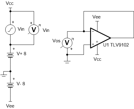 Figure 2-8 Power Supply Rejection
Ratio (PSRR+) Test Circuit
 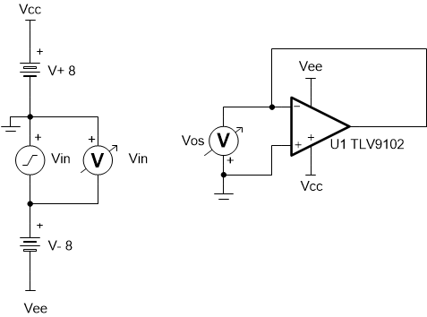 Figure 2-9 Power Supply Rejection
Ratio (PSRR-) Test Circuit
Figure 2-9 Power Supply Rejection
Ratio (PSRR-) Test CircuitCheck the DC operating point to verify that the op amp is operating in the linear region. When modeled correctly, the pole and zero location should match the graphs in the data sheet. Parasitic and higher-order effects at higher frequencies are problematic and cause some deviation from data sheet curves and the measured simulation characteristics in that region. Figure 2-10 shows the simulated PSRR+ and PSRR- results for TLV9102. Figure 2-11 shows the data sheet plot for CMRR, PSRR+, and PSRR- for TLV9102. For a more complete simulation test analysis; please refer to the following EDN article, authored by Ian Williams. This circuit may be simulated by downloading the AN1516 Test Circuits in either TINA-TI™ and PSpice® for TI.
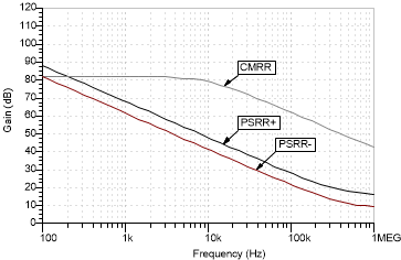 Figure 2-10 Simulated CMRR, PSRR+,
PSRR- for TLV9102
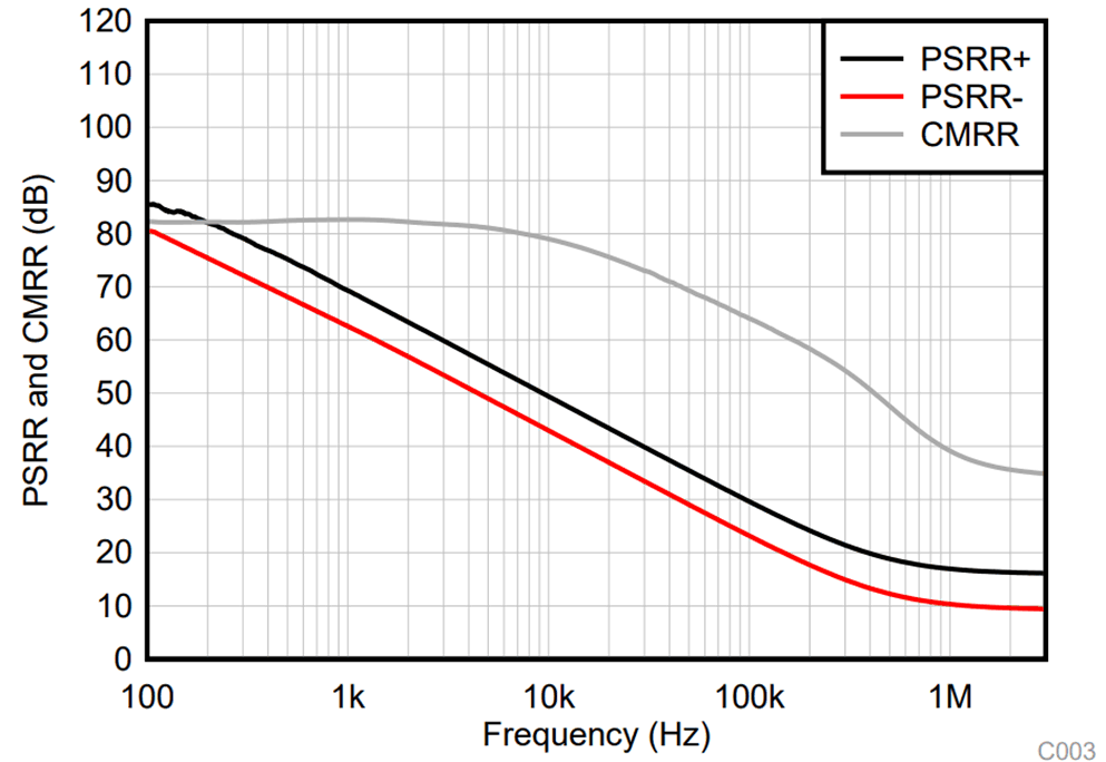 Figure 2-11 Data sheet Graph of CMRR,
PSRR+, PSRR- for TLV9102