SNOA475F October 2016 – September 2020 LMV791
- Trademarks
- 1Introduction
-
2What Parameters Should Be Tested?
- 2.1 Open-Loop Gain (AOL) and Phase Margin
- 2.2 Slew Rate
- 2.3 Common-Mode Rejection Ratio (CMRR) and Power Supply Rejection Ratio (PSRR)
- 2.4 Open-Loop Output Impedance (Zo)
- 2.5 Voltage Noise (en)
- 2.6 Current Noise (in)
- 2.7 Input Offset Voltage (VOS), Input Bias Current (Ib), and Quiescent Current (IQ)
- 2.8 Output Voltage Versus Output Current (Claw Curve)
- 2.9 Overload Recovery Time (tOR)
- 2.10 Common-mode Input Capacitance (CCM) and Common-mode Differential Capacitance (CDIFF)
- 2.11 Overshoot and Transient Response
- 2.12 Common-Mode Voltage Range (CMVR)
- 3Conclusion
- Revision History
2.1 Open-Loop Gain (AOL) and Phase Margin
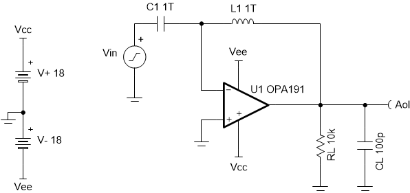
The open-loop gain versus frequency is important because it shows the DC gain, the dominant pole, the unity gain bandwidth and the phase margin. Figure 2-1 shows the circuit to test Open Loop Gain and Phase Margin Test Circuit. At DC, the capacitor is open and the inductor is short creating a feedback loop from output to inverting input of the op amp. At higher frequencies, the capacitor is a short and the inductor is open, this places the op amp in an open loop configuration. The capacitor and inductor values are chosen to be large to provide an early roll off [as seen in the formula below (1)] so that even if the op amp tested has a very low frequency dominant pole, the simulation shows a smooth transition and 20 dB per decade roll off. For more information on performing op amp stability analysis, please refer to the Texas Instruments Precision Labs video series on stability.

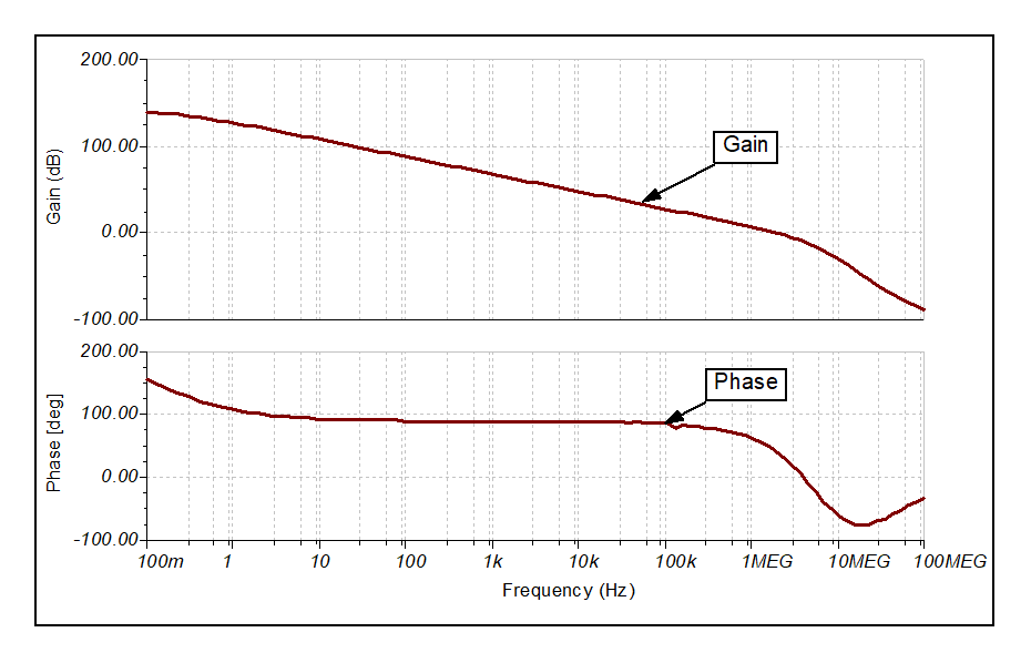
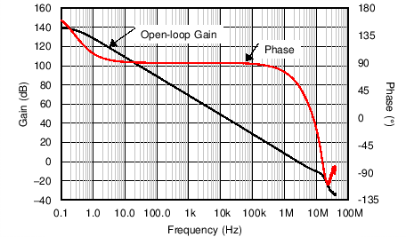
When testing open-loop gain and phase, the user should choose an upper frequency limit that goes beyond the unity-gain bandwidth of the amplifier. In the example provided, the unity-gain bandwidth of OPA191 is 2.5 MHz, Figure 2-2 shows the simulated AOL plot for OPA191 and Figure 2-3 shows the data sheet AOL plot for OPA191.
When using rail-to-rail output models, it is important to use the test circuit with the same load (RL and CL) indicated in the data sheet, otherwise the result might not reflect the actual amplifier’s capabilities. This is especially true about the DC gain (in consideration with formula 2). In the example provided, the OPA191 data sheet specifies an RL of 10 kΩ and CL of 100 pF.

For a more complete simulation test analysis, please refer to the following EDN article, authored by Ian Williams. This circuit may be simulated by downloading the AN1516 Test Circuits in either TINA-TI™ or PSpice® for TI.
 Figure 2-1 Open-Loop Gain and Phase
Margin Test Circuit
 Figure 2-2 Simulated Open-Loop Gain
and Phase for OPA191
 Figure 2-3 Data sheet Graph of Open
Loop Gain and Phase for OPA191