SNVU621D May 2019 – July 2021 LM61440 , LM61440-Q1 , LM61460 , LM61460-Q1
5 Board Layout
Figure 5-1 through Figure 5-6 show the board layout for the LM61460-Q1 EVM. The EVM offers resistors, capacitors, and test points to configure the following:
- Output voltage
- Precision enable pin
- Set frequency
- External clock synchronization
The 14-pin Hotrod package offers a very small size and low-noise solution. The PCB consists of a 4-layer design. There are 2-oz copper planes on the top and bottom and 1-oz copper mid-layer planes to dissipate heat with an array of thermal vias to connect to all four layers.
Test points have been provided for ease of use to connect the power supply and required load, and to monitor critical signals.
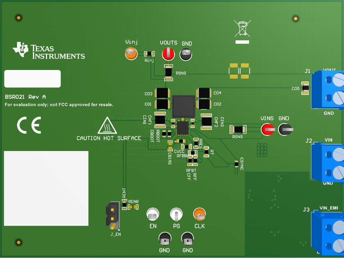 Figure 5-1 Top 3D
View
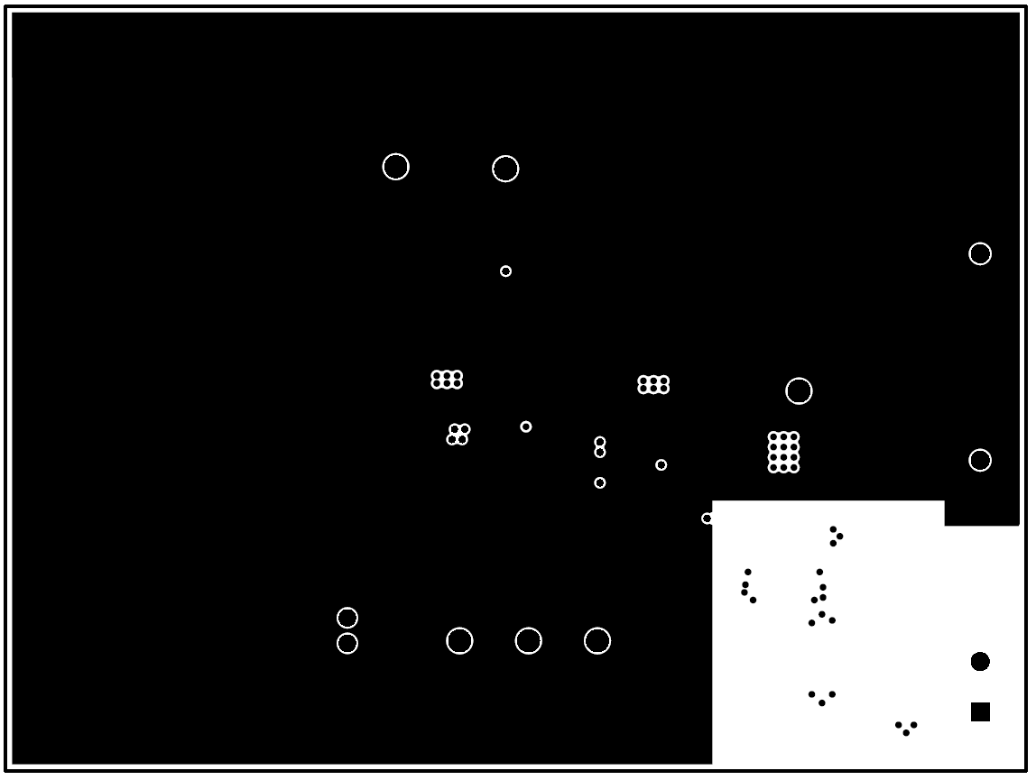 Figure 5-3 Signal Layer 1
- Ground Plane
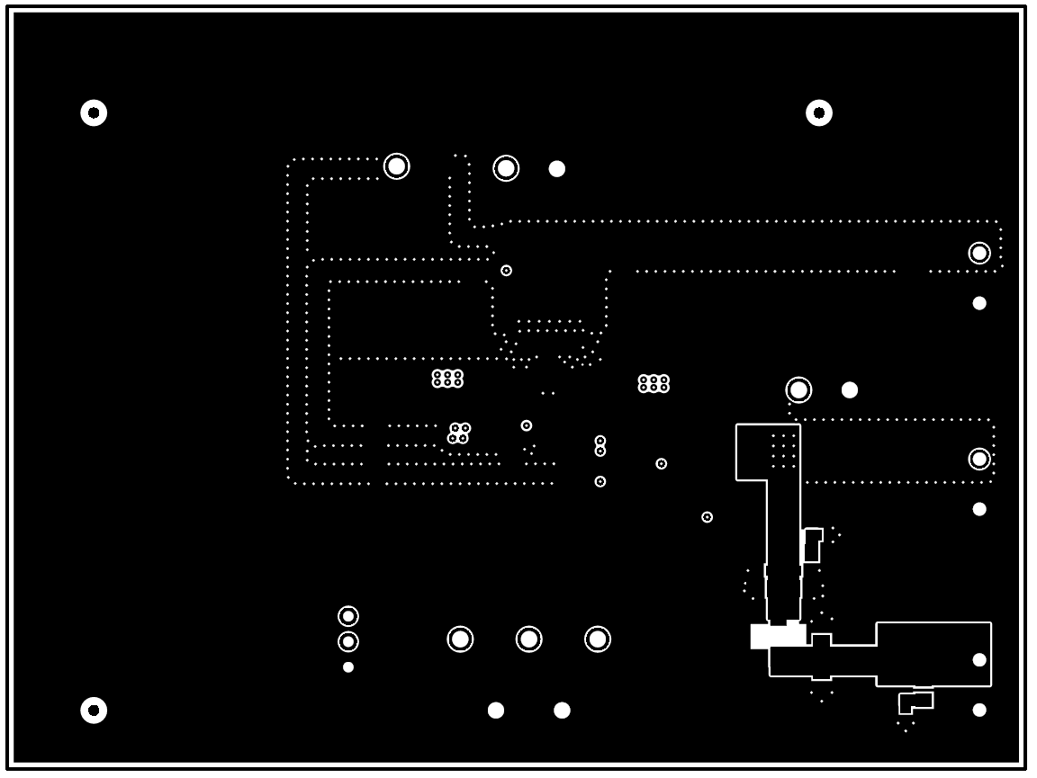 Figure 5-5 Bottom
Layer
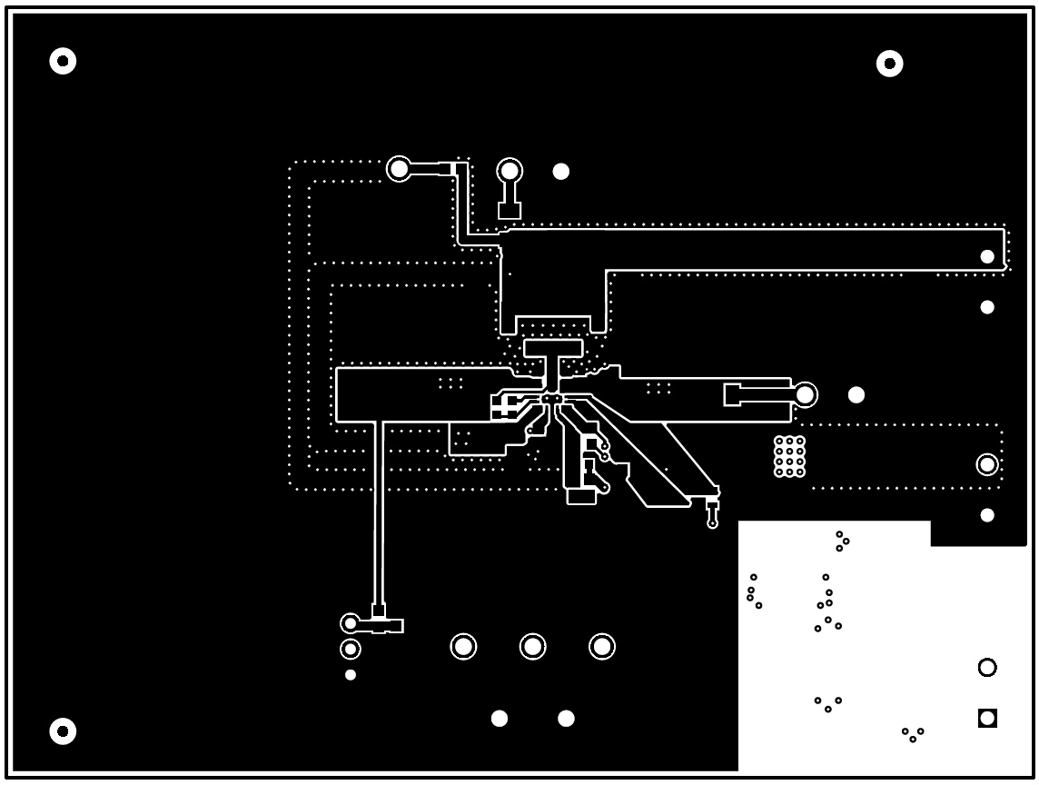 Figure 5-2 Top
Layer
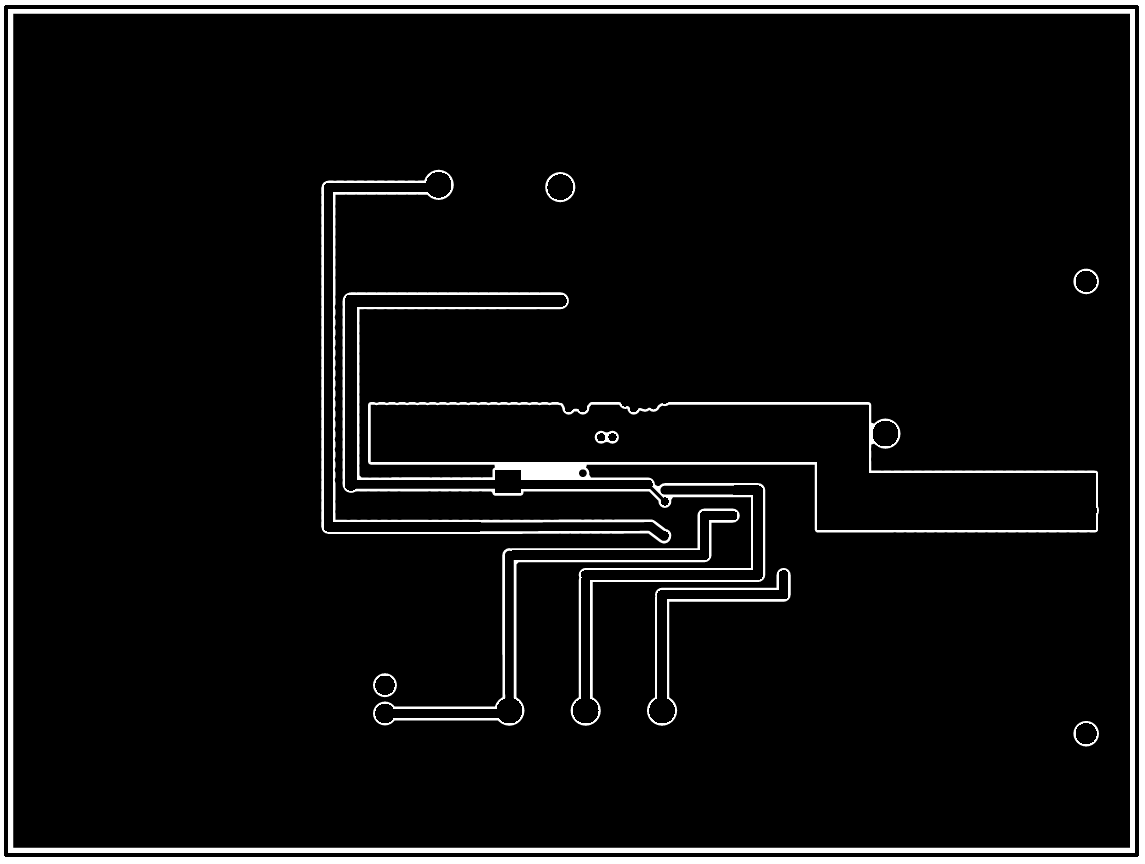 Figure 5-4 Signal Layer 2
- Routing
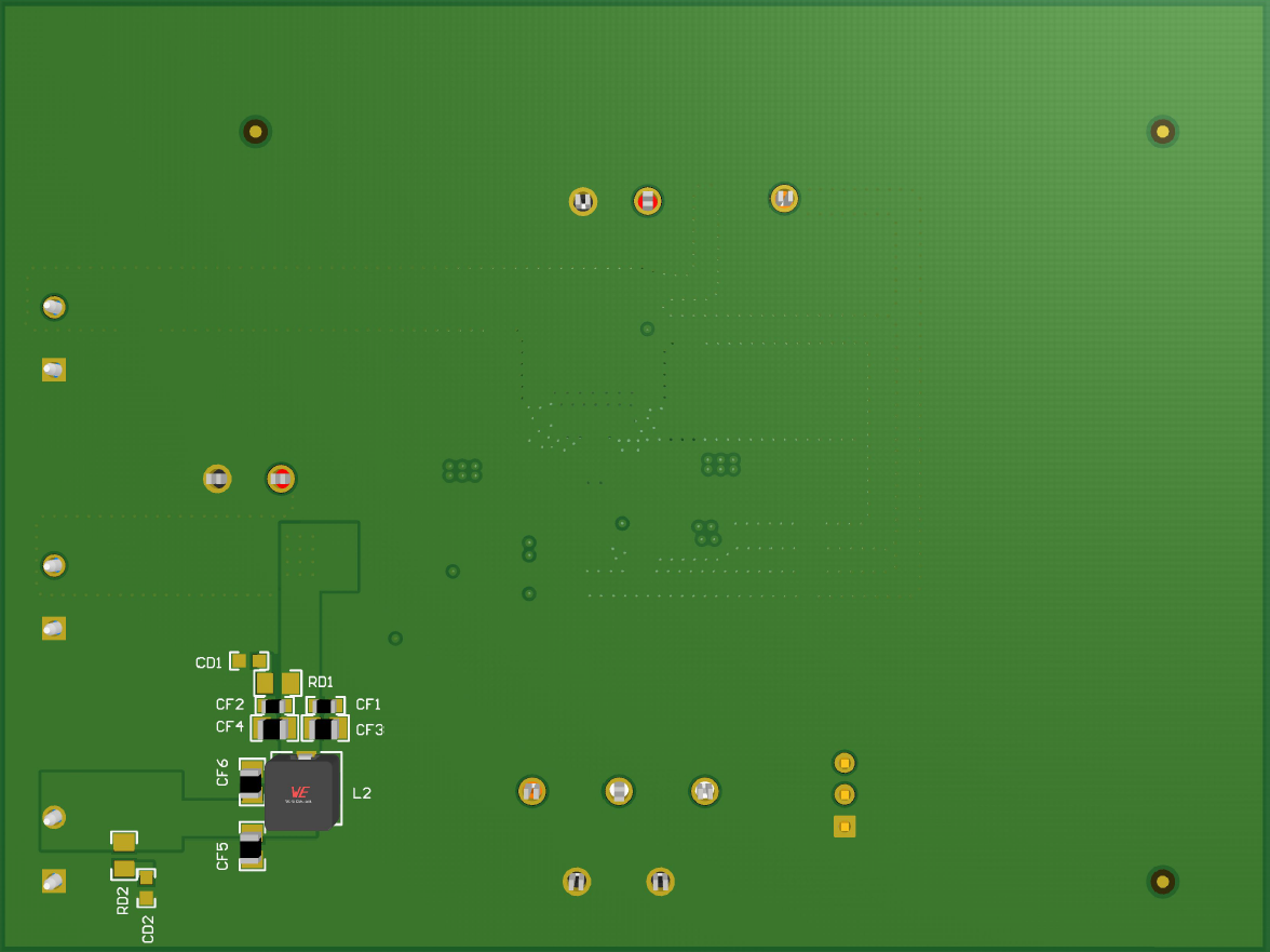 Figure 5-6 Bottom 3D view