SPRACY3 June 2021 F29H850TU , F29H859TU-Q1 , TMS320F280023C , TMS320F280025C , TMS320F280025C-Q1 , TMS320F280040C-Q1 , TMS320F280041C , TMS320F280041C-Q1 , TMS320F280048C-Q1 , TMS320F280049C , TMS320F280049C-Q1 , TMS320F28076 , TMS320F28379D , TMS320F28379D-Q1 , TMS320F28379S , TMS320F28386D , TMS320F28386D-Q1 , TMS320F28386S , TMS320F28386S-Q1 , TMS320F28388D , TMS320F28388S , TMS320F28P650DH , TMS320F28P650DK , TMS320F28P650SH , TMS320F28P650SK , TMS320F28P659DH-Q1 , TMS320F28P659DK-Q1 , TMS320F28P659SH-Q1
6 Test Results
The delayed protection scheme with CLB has been validated with the LaunchPad LAUNCHXL-F280049C. In the given example code, changing positive_cycle to 1 or 0 to decide positive cycle or negative cycle operation; changing EPWM8_Cmpa value to simulate different time scale for the trip signal; changing trip_within_one_cycle to simulate different types of trip signals, including sustaining within or across one EPWM cycle. It has been validated for single phase NPC inverter and extending to 3 phase NPC inverter.
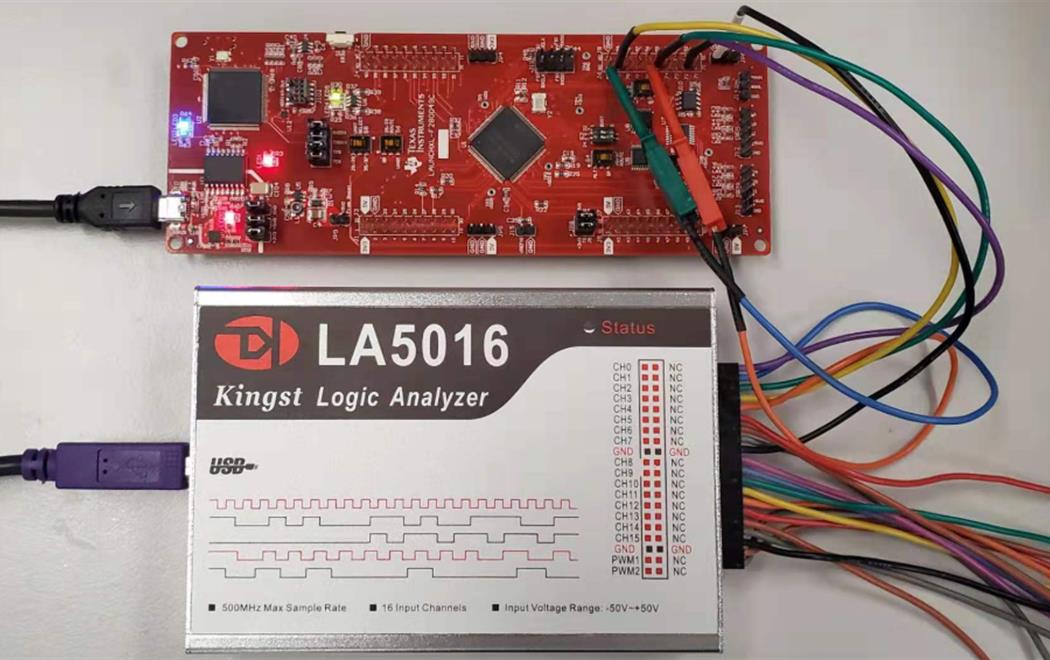
The test results were measured with Kingst Logic Analyzer, as shown in Figure 6-1. And the related pin mapping information in this example is shown in Table 6-1.
 Figure 6-1 Test Platform Set Up
| Signal Name | Description | Connection to the LaunchPad | |
|---|---|---|---|
| EPWM8A | Trip Event | GPIO-14 | |
| EPWM1A | Control signal for S1 | GPIO-00 | |
| EPWM2B | Control signal for S2 | GPIO-03 | |
| EPWM1B | Control signal for S3 | GPIO-01 | |
| EPWM2A | Control signal for S4 | GPIO-02 | |
| EPWM5A | Control signal for S1 | See the 3rd phase for 3 phase NPC inverter | GPIO-08 |
| EPWM6B’ | Control signal for S2, CLB output | GPIO-17 | |
| EPWM5B’ | Control signal for S3, CLB output | GPIO-16 | |
| EPWM6A | Control signal for S4 | GPIO-10 | |
| EPWM6B | Original EPWM6B signal | GPIO-11 | |
| EPWM5B | Original EPWM5B signal | GPIO-09 | |
Figure 6-2 shows the condition of trip during positive cycle, where EPWM1A starts CBC protection right at the trip low moment, while EPWM1B turns low after a delay of 1.035 μs. It was well matched with the defined 1 µs, considering the extra timing required by the internal hardware logic. Figure 6-3 shows the trip signal during negative cycle, where the delayed protection logic works as expected.
 Figure 6-2 Trip Signal During Positive
Cycle
 Figure 6-3 Trip Signal During Negative
Cycle
Figure 6-3 Trip Signal During Negative
CycleFigure 6-4 shows the waveforms of EPWM5 and EPWM6 in normal operation during positive cycle, with both rising edge delay and falling edge delay of 1 µs defined. And EPWM5B and EPWM6B measured are not the initial EPWMxB, but the signals after the CLB module. It shows that the dead time between EPWM5A and EPWM5B is 1.025 μs and 0.975 μs, thus the delay induced by the CLB module should be acceptable.
 Figure 6-4 PWM5 and PWM6 in Normal Operation
During Positive Cycle
 Figure 6-5 and Figure 6-6 show the waveform of EPWM5 and EPWM6 with trip signal during positive cycle and negative cycle, respectively.
 Figure 6-5 PWM5 and PWM6 With Trip Signal
During Positive Cycle
 Figure 6-6 Trip Across One PWM Period During
Negative Cycle