SPRADD4 October 2023 AM625SIP
9 SerDes Interfaces
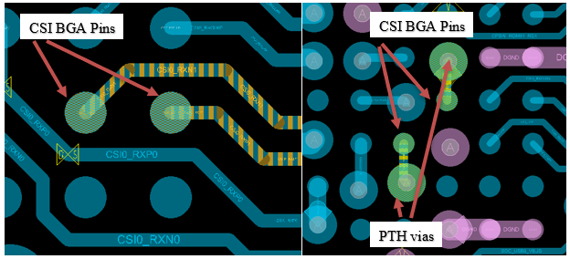
The package BGA ball map is also arranged to support routing the highest priority interfaces first. Therefore, the SerDes CSI interfaces are located on the outer two rings. The differential receive pair should be routed away from the SoC on the top layer leaving a gap without blocking vias. The lanes located on inner BGA rows require vias to escape as a differential pair on the bottom or on an interior layer. The VCA facilitates this for inner rows. See Figure 9-1 for an example of the escape of the SerDes signals on the AM62XSiP board on the top layer and on an inner layer. Wide traces can limit the signal loss but could violate the impedance requirements. For more detailed information on routing Serdes signals, refer to High-Speed Interface Layout Guidelines.
 Figure 9-1 Serdes CSI Escapes for TOP Layer (Left) and Inner Layer (Right)