SPRADD4 October 2023 AM625SIP
12 Summary
The via channels have been carefully co-designed to ensure escapes for all signals and power while meeting the respective signal and power integrity goals for each interface. A summary of all via channel arrays and vias for the different power supply nets is shown in Table 12-1.
Table 12-1 Via Channel Summary
| Net | #Pins | #Vias for BGA Escape |
|---|---|---|
| VDD_CORE | 17 | 21 |
| VDDR_CORE | 8 | |
| VDD_CANUART | 1 | |
| VDDA_CORE_USB | 1 | |
| VDDA_CORE_CSIRX0 | 1 | |
| VDDS_DDR | 5 | 2 |
| VDDS_DDR_MEM | 12 | 5 |
| VDDSHV0 | 2 | 8 |
| VDDSHV2 | 2 | |
| VDDSHV3 | 4 | |
| VDDSHV_MCU | 2 | |
| VDDSHV_CANUART | 1 | |
| VDDA_3P3_USB | 1 | |
| VMON_3P3_SOC | 1 | |
| VDDSHV1 | 2 | 3 |
| VDDSHV4 | 1 | |
| VDDSHV6 | 1 | |
| VMON_1P8_SOC | 1 | |
| VDDSHV5 | 1 | 1 |
| VDDS_OSC0 | 1 | 11 |
| VDDA_TEMP[0:1] | 2 | |
| VDDA_PLL[0:2] | 3 | |
| VDDA_MCU | 1 | |
| VDDA_1P8_OLDI0 | 2 | |
| VDDA_1P8_CSIRX0 | 1 | |
| VDDA_1P8_USB | 1 | |
| VDDS_MEM_1P8 | 2 |
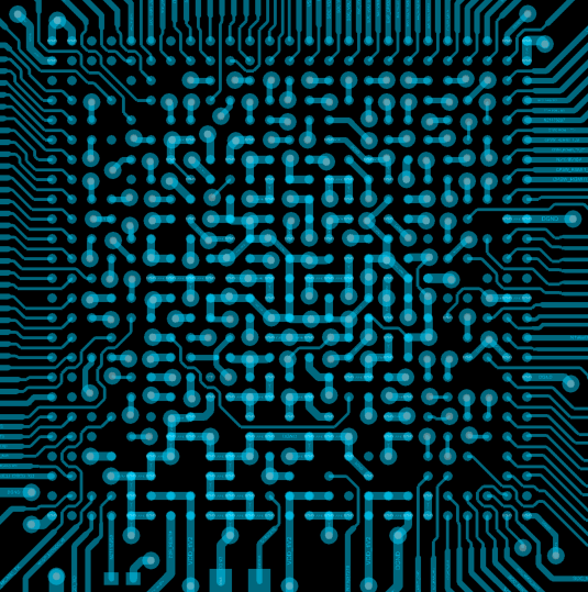
A picture with AM62xSiP with all signals and power escaped is shown in Figure 12-1.
 Figure 12-1 AM62xSiP with Complete Signal and Power Escapes