SPRADD9 September 2023 TMS320F2800132 , TMS320F2800133 , TMS320F2800135 , TMS320F2800137 , TMS320F2800152-Q1 , TMS320F2800153-Q1 , TMS320F2800154-Q1 , TMS320F2800155 , TMS320F2800155-Q1 , TMS320F2800156-Q1 , TMS320F2800157 , TMS320F2800157-Q1 , TMS320F280021 , TMS320F280021-Q1 , TMS320F280023 , TMS320F280023-Q1 , TMS320F280023C , TMS320F280025 , TMS320F280025-Q1 , TMS320F280025C , TMS320F280025C-Q1 , TMS320F280033 , TMS320F280034 , TMS320F280034-Q1 , TMS320F280036-Q1 , TMS320F280036C-Q1 , TMS320F280037 , TMS320F280037-Q1 , TMS320F280037C , TMS320F280037C-Q1 , TMS320F280038-Q1 , TMS320F280038C-Q1 , TMS320F280039 , TMS320F280039-Q1 , TMS320F280039C , TMS320F280039C-Q1 , TMS320F280040-Q1 , TMS320F280040C-Q1 , TMS320F280041 , TMS320F280041-Q1 , TMS320F280041C , TMS320F280041C-Q1 , TMS320F280045 , TMS320F280048-Q1 , TMS320F280048C-Q1 , TMS320F280049 , TMS320F280049-Q1 , TMS320F280049C , TMS320F280049C-Q1
1.3 ePWM Configurations Proposed
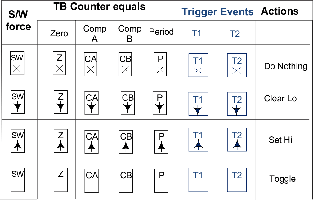
Combining the above requirements, the below ePWM configurations are proposed, shown in Figure 1-6. Take ePWM1 as example, ePWM1A is defined to set high at ZREO event, and clear low at CMPA or T1 event. T1 event, which is triggered by the comparator for the inductor current, is selected to clear low ePWM1A at the overcurrent condition, in replace of the traditional CBC scheme. As shown in Figure 1-7, with the latest Type 4 ePWM, T1 and T2 events, sourcing from comparator, trip or sync events, can also generate actions through action qualifier (AQ) submodule. More details regarding new T1/T2 features can refer to TRM. Since the AQ submodule is before the dead band (DB) submodule, it is natural to enable the rising edge delay and falling edge delay for ePWM1A and ePWM1B, respectively, with active high complementary (AHC) mode. As shown in the 1st and 2nd cycle in Figure 1-6, it covers the normal operation and the overcurrent conditions. For the reverse current control, it can be simplified to use the traditional CBC protection based on the zero current detection (ZCD) event, which takes effect for both ePWM1A and ePWM1B. As shown in the 3rd cycle, ePWM1A output is already low during the negative current event, so it can be set with the same action as ePWM1B, regardless of the VAC polarity.
 Figure 1-6 Basic ePWM Configurations
Block Diagram
 Figure 1-7 Action-Qualifier Actions for
ePWMxA and ePWMxB Outputs
Figure 1-7 Action-Qualifier Actions for
ePWMxA and ePWMxB OutputsSince the active FET and sync FET role is exchanged under positive cycle and negative cycle, the related PWM control signals are required to exchange also, which can be support by the DB submodule of Type 4 ePWM directly. As shown in Figure 1-8, S6 and S7 are used to swap ePWMxA and ePWMxB output. And the added red arrows also indicate the detailed settings inside the DB submodule.
 Figure 1-8 Dead Band Submodule Block
Diagram
Figure 1-8 Dead Band Submodule Block
DiagramIn order to better demonstrate how to leverage the T1 event together with CMPSS for the totem pole PFC configurations, the below example codes are provided. In this example, CMPSS1_H is selected as the source for TRIP4 input through ePWM X-Bar. Note that only the T1 event related configurations are shown, and other ePWM settings can refer to the example projects in C2000WARE.
    XBAR_setEPWMMuxConfig(XBAR_TRIP4, XBAR_EPWM_MUX00_CMPSS1_CTRIPH);
    XBAR_enableEPWMMux(XBAR_TRIP4, XBAR_MUX00);

    // assign DCAL for TRIP4
    EPWM_selectDigitalCompareTripInput(base,EPWM_DC_TRIP_TRIPIN4,EPWM_DC_TYPE_DCAL);

    EPWM_setTripZoneDigitalCompareEventCondition(base,EPWM_TZ_DC_OUTPUT_A2,EPWM_TZ_EVENT_DCXL_HIGH);

    // DCAEVT2 = DCAEVT2 (not filtered)

    EPWM_setDigitalCompareEventSource(base, EPWM_DC_MODULE_A,
                                      EPWM_DC_EVENT_2,
                                      EPWM_DC_EVENT_SOURCE_ORIG_SIGNAL);

    // Select DCAEVT2 event as AQ T1 source
    EPWM_setActionQualifierT1TriggerSource(base, EPWM_AQ_TRIGGER_EVENT_TRIG_DCA_2);

    // This is to avoid impact of high impedance state
    EPWM_setTripZoneAction(base, EPWM_TZ_ACTION_EVENT_DCAEVT2, EPWM_TZ_ACTION_DISABLE);

    //During the normal condition
    EPWM_setActionQualifierAction(base,EPWM_AQ_OUTPUT_A,EPWM_AQ_OUTPUT_HIGH, EPWM_AQ_OUTPUT_ON_TIMEBASE_ZERO);
    EPWM_setActionQualifierAction(base,EPWM_AQ_OUTPUT_A,EPWM_AQ_OUTPUT_LOW, EPWM_AQ_OUTPUT_ON_TIMEBASE_UP_CMPA);
    //set T1 action for EPWM1A during CBC protection
   EPWM_setActionQualifierAction(base,EPWM_AQ_OUTPUT_A,EPWM_AQ_OUTPUT_LOW, EPWM_AQ_OUTPUT_ON_T1_COUNT_UP);