SPRUJ40C may 2022 – may 2023
- 1
- Abstract
- Trademarks
- 1EVM Revisions and Assembly Variants
-
2System Description
- 2.1 Key Features
- 2.2 Functional Block Diagram (SK-AM62 and SK-AM62B)
- 2.3 Functional Block Diagram (SK-AM62-P1 and SK-AM62B-P1)
- 2.4 AM62x SKEVM Interface Mapping
- 2.5 Power ON/OFF Procedures
- 2.6
Peripheral and Major Component
Description
- 2.6.1 Clocking
- 2.6.2 Reset
- 2.6.3 OLDI Display Interface
- 2.6.4 CSI Interface
- 2.6.5 Audio Codec Interface
- 2.6.6 HDMI Display Interface
- 2.6.7 JTAG Interface
- 2.6.8 Test Automation Header
- 2.6.9 UART Interface
- 2.6.10 USB Interface
- 2.6.11 Memory Interfaces
- 2.6.12 Ethernet Interface
- 2.6.13 GPIO Port Expander
- 2.6.14 GPIO Mapping
- 2.6.15 Power
- 2.6.16 AM62x SKEVM User Setup/Configuration
- 2.6.17 Expansion Headers
- 2.6.18 Interrupt
- 2.6.19 I2C Address Mapping
-
3Known Issues and Modifications
- 3.1 Issue 1 - HDMI/DSS Incorrect Colors on E1
- 3.2 Issue 2 - J9 and J10 Header Alignment on E1
- 3.3 Issue 3 - USB Boot descoped on E1
- 3.4 Issue 4 - OLDI Connector Orientation and Pinout
- 3.5 Issue 5 - Bluetooth descoped on E2 EVMs
- 3.6 Issue 6 - Ethernet PHY CLK Skew Default Strapping Changes
- 3.7 Issue 7 - TEST_POWERDOWN changes
- 3.8 Issue 8 - MMC1_SDCD spurious interrupts
- 3.9 Issue 9 - PD Controller I2C2 IRQ Not Pinned Out
- 3.10 Issue 10 - INA Current Monitor Adress Changes
- 3.11 Issue 11 - Test Automation I2C Buffer Changes
- Regulatory Compliance
- Revision History
2.6.16.2 Boot Modes
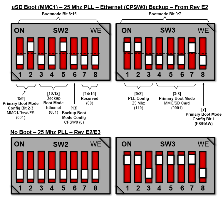
The boot mode for the SK EVM board is defined by two banks of switches SW1 and SW2 or by the I2C buffer connected to the Test automation connector. This allows for AM62x SoC Boot mode control by either the user (DIP Switch Control) or by the Test Automation connector.
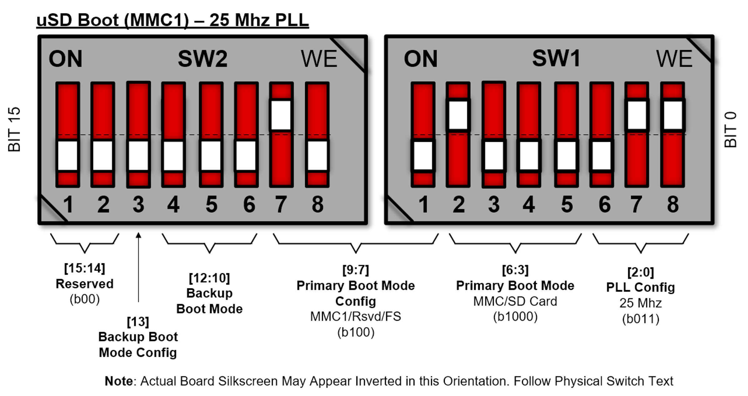
All the bits of switch (SW1 and SW2) have week pull down resistor and a strong pull up resistor as shown in below picture. Note that OFF setting provides a low logic level (‘0’) and an ON setting provides a high logic level (‘1’). Figure 2-17 Bootmode Switch Configuration
for SD Boot (From E2)
 Figure 2-18 Bootmode Switch Configuration
for SD Boot (E1)
Figure 2-18 Bootmode Switch Configuration
for SD Boot (E1)The boot mode pins of the SoC have associated alternate functions during normal operation. Hence isolation is provided using Buffer IC’s to cater for alternate pin functionality. The output of the buffer is connected to the bootmode pins on the AM62x and the output is enabled when the bootmode is needed during a reset cycle. The input to the buffer is connected to the DIP switch circuit and to the output of an I2C buffer set by the test automation circuit. If the test automation circuit is going to control the bootmode, all the switches will manually be set to the OFF position. The bootmode buffer should be powered by an always ON power supply to ensure that the bootmode remains present even if the SoC power is cycled.
Switch SW1 and SW2 bits [15:0] are used to set the SoC Boot mode.
The switch map to the boot mode functions is provided in the tables below.
| Bit 15 | Bit 14 | Bit 13 | Bit 12 | Bit 11 | Bit 10 | Bit 9 | Bit 8 | Bit 7 | Bit 6 | Bit 5 | Bit 4 | Bit 3 | Bit 2 | Bit 1 | Bit 0 |
|---|---|---|---|---|---|---|---|---|---|---|---|---|---|---|---|
| Reserved | Reserved | Backup Boot Mode Configuration | Backup Boot Mode | Primary Boot Mode Configuration | Primary Boot Mode | PLL Configuration | |||||||||
- BOOT-MODE [0:2] – Denote system clock frequency for PLL configuration. By default, this bits are set for 25 MHz.
Table 2-18 gives details ON PLL reference clock selection.
| Bit 2 | Bit 1 | Bit 0 | PLL REF CLK (MHz) |
|---|---|---|---|
| OFF | OFF | OFF | RSVD |
| OFF | OFF | ON | RSVD |
| OFF | ON | OFF | 24 |
| OFF | ON | ON | 25 |
| ON | OFF | OFF | 26 |
| ON | OFF | ON | RSVD |
| ON | ON | OFF | RSVD |
| ON | ON | ON | RSVD |
- BOOT-MODE [3:6] – This provides primary boot mode configuration to select the requested boot mode after POR, that is, the peripheral/memory to boot from. Table 2-19 provides primary boot device selection details.
| Bit 6 | Bit 5 | Bit 4 | Bit 3 | Primary Boot Device Selected |
|---|---|---|---|---|
| OFF | OFF | OFF | OFF | Serial NAND |
| OFF | OFF | OFF | ON | OSPI |
| OFF | OFF | ON | OFF | QSPI |
| OFF | OFF | ON | ON | SPI |
| OFF | ON | OFF | OFF | Ethernet RGMII1 |
| OFF | ON | OFF | ON | Ethernet RMII1 |
| OFF | ON | ON | OFF | I2C |
| OFF | ON | ON | ON | UART |
| ON | OFF | OFF | OFF | MMC/SD card |
| ON | OFF | OFF | ON | eMMC |
| ON | OFF | ON | OFF | USB0 |
| ON | OFF | ON | ON | GPMC NAND |
| ON | ON | OFF | OFF | GPMC NOR |
| ON | ON | OFF | ON | Rsvd |
| ON | ON | ON | OFF | xSPI |
| ON | ON | ON | ON | No boot/Dev Boot |
- BOOT-MODE [10:12] – Select the backup boot mode, that is, the peripheral/memory to boot from, if primary boot device failed.
Table 2-20 provides backup boot mode selection details.
| Bit 12 | Bit 11 | Bit 10 | Backup Boot Device Selected |
|---|---|---|---|
| OFF | OFF | OFF | None (No backup mode) |
| OFF | OFF | ON | USB |
| OFF | ON | OFF | Reserved |
| OFF | ON | ON | UART |
| ON | OFF | OFF | Ethernet |
| ON | OFF | ON | MMC/SD |
| ON | ON | OFF | SPI |
| ON | ON | ON | I2C |
- BOOT-MODE [9:7] – These pins provide optional settings and are used in conjunction with the primary boot device selected.
Table 2-21 gives primary boot media configuration details.
| Bit 9 | Bit 8 | Bit 7 | Boot Device |
|---|---|---|---|
| Reserved | Read Mode 2 | Read Mode 1 | Serial NAND |
| Speed | Iclk | Csel | OSPI |
| Reserved | Iclk | Csel | QSPI |
| Reserved | Mode | Csel | SPI |
| Clkout | Delay | Link stat | Ethernet RGMII |
| Clkout | Clk src | Reserved | Ethernet RMII |
| Bus Reset | Reserved | Addr | I2C |
| Reserved | Reserved | UART | |
| Port | Reserved | Fs/raw | MMC/ SD card |
| Reserved | voltage | eMMC | |
| Reserved | Mode | Lane swap | USB0 |
| Reserved | GPMC NAND | ||
| Reserved | GPMC NOR | ||
| Reserved | Reserved | ||
| SFDP | Read Cmd | Mode | xSPI |
| Reserved | No/Dev | No boot/Dev Boot | |
- BOOT-MODE [13] – These pins provide optional settings and are used in conjunction with the backup boot device devices. Switch SW2.6 when ON sets 1 and sets 0 if OFF, see the device-specific TRM.
- BOOT-MODE [14:15] – Reserved.
Table 2-22 provides backup boot media configuration options.
| Bit 13 | Boot Device |
|---|---|
| Reserved | None |
| Mode | USB |
| Reserved | Reserved |
| Reserved | UART |
| IF | Ethernet |
| Port | MMC/SD |
| Reserved | SPI |
| Reserved | I2C |