SPRUJ40C may 2022 – may 2023
- 1
- Abstract
- Trademarks
- 1EVM Revisions and Assembly Variants
-
2System Description
- 2.1 Key Features
- 2.2 Functional Block Diagram (SK-AM62 and SK-AM62B)
- 2.3 Functional Block Diagram (SK-AM62-P1 and SK-AM62B-P1)
- 2.4 AM62x SKEVM Interface Mapping
- 2.5 Power ON/OFF Procedures
- 2.6
Peripheral and Major Component
Description
- 2.6.1 Clocking
- 2.6.2 Reset
- 2.6.3 OLDI Display Interface
- 2.6.4 CSI Interface
- 2.6.5 Audio Codec Interface
- 2.6.6 HDMI Display Interface
- 2.6.7 JTAG Interface
- 2.6.8 Test Automation Header
- 2.6.9 UART Interface
- 2.6.10 USB Interface
- 2.6.11 Memory Interfaces
- 2.6.12 Ethernet Interface
- 2.6.13 GPIO Port Expander
- 2.6.14 GPIO Mapping
- 2.6.15 Power
- 2.6.16 AM62x SKEVM User Setup/Configuration
- 2.6.17 Expansion Headers
- 2.6.18 Interrupt
- 2.6.19 I2C Address Mapping
-
3Known Issues and Modifications
- 3.1 Issue 1 - HDMI/DSS Incorrect Colors on E1
- 3.2 Issue 2 - J9 and J10 Header Alignment on E1
- 3.3 Issue 3 - USB Boot descoped on E1
- 3.4 Issue 4 - OLDI Connector Orientation and Pinout
- 3.5 Issue 5 - Bluetooth descoped on E2 EVMs
- 3.6 Issue 6 - Ethernet PHY CLK Skew Default Strapping Changes
- 3.7 Issue 7 - TEST_POWERDOWN changes
- 3.8 Issue 8 - MMC1_SDCD spurious interrupts
- 3.9 Issue 9 - PD Controller I2C2 IRQ Not Pinned Out
- 3.10 Issue 10 - INA Current Monitor Adress Changes
- 3.11 Issue 11 - Test Automation I2C Buffer Changes
- Regulatory Compliance
- Revision History
2.6.7 JTAG Interface
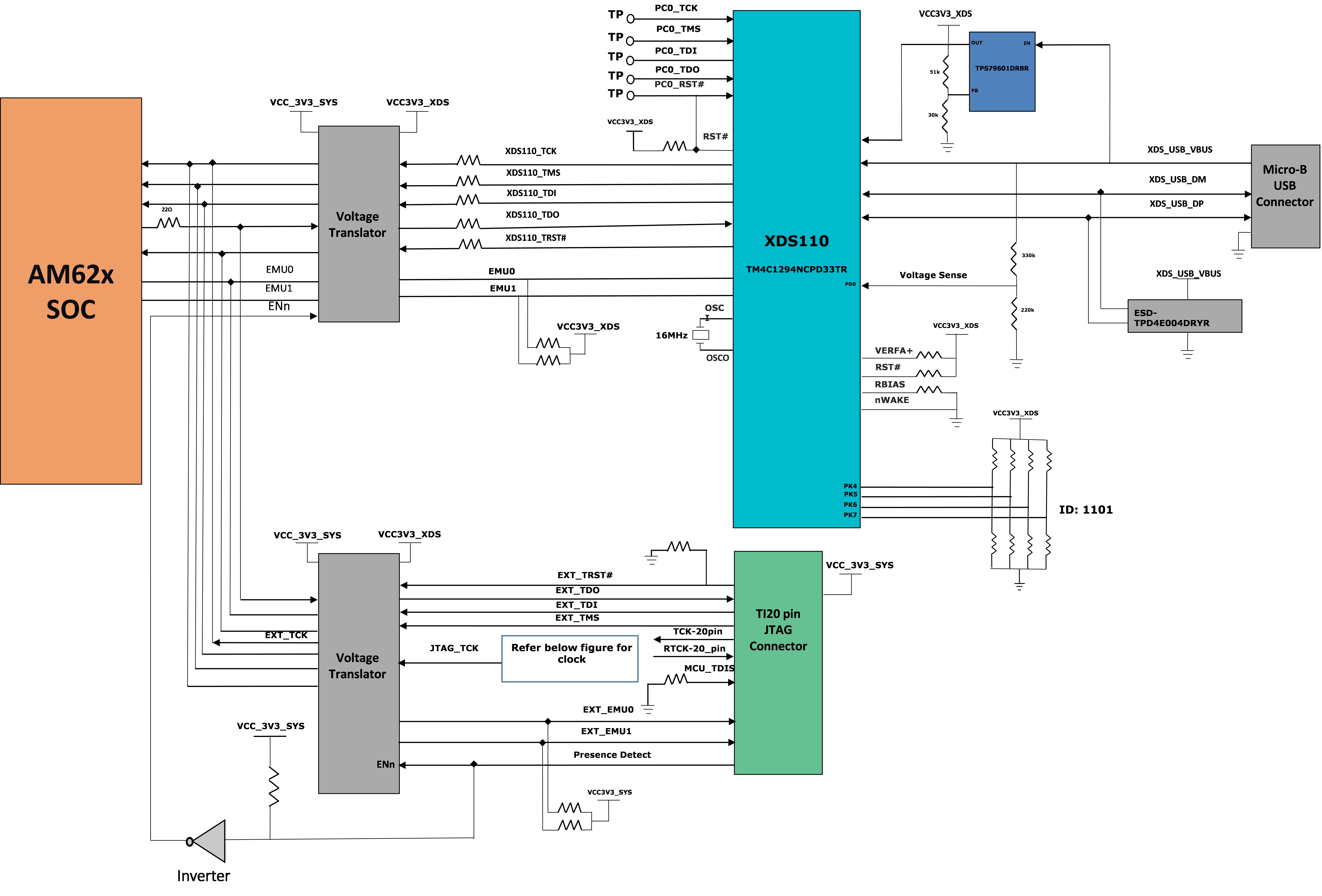
AM62x SKEVM board include XDS110 class on board emulation. The connection for the emulator uses an USB 2.0 micro-B connector and the circuit acts as a Bus powered USB device. The VBUS power from the connector will be used to power the emulation circuit such that connection to the emulator is not lost when the power to the SKEVM is removed. Voltage translation buffers are used to isolate the XDS110 circuit from the rest of the SKEVM.
Optionally, JTAG Interface on SKEVM is also provided through 20 Pin Standard JTAG cTI Header J17. This allows the user to connect an external JTAG Emulator Cable. Voltage translation buffers are used to isolate the JTAG signals from cTI header from the rest of the SKEVM. The output from the voltage translators from XDS110 Section and cTI Header Section are muxed and connected to AM62x JTAG Interface. If a connection to the cTI 20 Pin JTAG connector is sensed using a presence detect circuit, the mux will be set to route the 20 pin signals from the cTI connector to the AM62x SoC in place of the on-board emulation circuit.

The pin-outs of the cTI 20 pin JTAG connector are given in Table 2-7. A ESD protection part number TPD4E004 is provided on USB signals to steer ESD current pulses to VCC or GND. TPD4E004 protects against ESD pulses up to ±15-kV Human-Body Model (HBM) as specified in IEC 61000-4-2 and provides ±8-kV contact discharge and ±12- kV air-gap discharge.
| Pin No. | Signal |
|---|---|
| 1 | JTAG_TMS |
| 2 | JTAG_TRST# |
| 3 | JTAG_TDI |
| 4 | JTAG_TDIS |
| 5 | VCC3V3_SYS |
| 6 | NC |
| 7 | JTAG_TDO |
| 8 | SEL_XDS110_INV |
| 9 | JTAG_cTI_RTCK |
| 10 | DGND |
| 11 | JTAG_cTI_TCK |
| 12 | DGND |
| 13 | JTAG_EMU0 |
| 14 | JTAG_EMU1 |
| 15 | JTAG_EMU_RSTn |
| 16 | DGND |
| 17 | NC |
| 18 | NC |
| 19 | NC |
| 20 | DGND |