SSZT235 october 2020 AMC3301 , AMC3301-Q1 , AMC3302 , AMC3306M25 , AMC3330 , AMC3330-Q1
It is necessary everywhere – to protect humans, provide noise immunity and handle ground potential differences between subsystems. You design for it in applications such as motor drives, solar inverters, DC charging (pile) stations, industrial robots, uninterruptible power supplies, traction inverters, onboard chargers and DC/DC converters.
I’m referring, of course, to galvanic isolation.
Systems, like the ones I mentioned above, require the transfer of current and voltage information from one power domain to the other over an isolation barrier for monitoring and control purposes. How do you transfer analog information over the isolation barrier? The answer lies in isolated amplifiers and isolated analog-to-digital converters (ADCs), the latter of which are also known as isolated delta-sigma modulators.
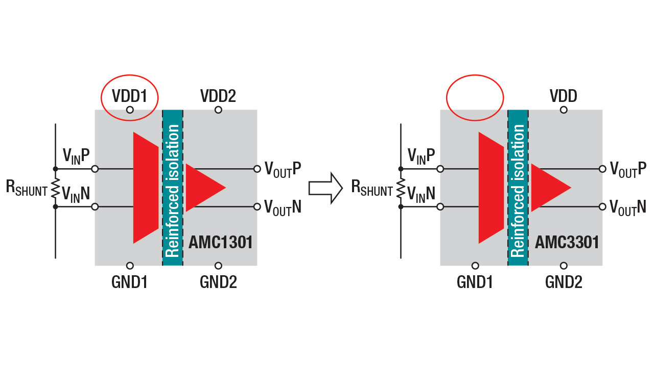
One key challenge when designing these systems is figuring out how to provide power supplies to the isolated amplifier or ADC. Traditionally, they need two power supplies: one on the high-side and one on the low-side (shown in the left image of Figure 1 as VDD1 and VDD2, respectively). The low side is often powered from the same supply that powers the digital controller, but many systems do not have a power supply readily available on the high side. This means that you’ll have to design a discrete isolated power supply on the high side (this will increase solution size, bill of materials [BOM] count, and solution cost), which increases complexity in the design and printed circuit board (PCB) layout.
To address this design challenge, we developed a family of isolated amplifiers and ADCs that can operate using a single supply on the low side. Figure 1 shows the difference between standard isolated converters that need two power supplies (on the left) and the AMC3301 family, which can operate with single supply (on the right).
 Figure 1 Traditional isolated amplifier
vs. isolated amplifier with a single supply
Figure 1 Traditional isolated amplifier
vs. isolated amplifier with a single supplyThese new devices include a fully integrated DC/DC converter stage to generate the high-side supply internally. The architecture of this DC/DC converter is optimized to source as much as 1 mA of additional DC current from the high-side low-dropout regulator (LDO) output pin (usually denoted as HLDOOUT) for auxiliary circuitry, such as an active filter, a pre-amplifier or a comparator.
| High accuracy for shunt-based current sensing. | |

AMC3301 |
Learn more about the AMC3301 precision reinforced-isolated amplifier with integrated DC/DC converter. |
How a single-supply operation can simplify designs
The advantages of single-supply operation include:
- A smaller solution size, reduced bill of materials (BOM) and lower system cost. An integrated DC/DC converter eliminates the need for discrete power supplies, such as a dedicated isolated power supply and the combination of dedicated transformer, transformer driver and LDO. This integration enables you to create compact system designs for space-constrained applications, and can help you reduce BOM count and lower system costs.
- The opportunity to simplify your design and layout. Not having to worry about the availability of the high-side supply makes it easier to design high-accuracy shunt-based current and voltage sensing. You can:
- Achieve higher reuse with a modular PCB design by eliminating the need for a centralized power supply.
- Enable two-layer board designs with fewer traces and less power routing.
- Remove design complexity when doing phase-to-phase voltage measurements in a multiphase system without a common neutral. You can eliminate discrete isolated power supplies that would otherwise be needed.
- Flexibility in shunt placement. In traditional architectures, the existence of a power supply on the high side dictates the shunt placement, which may lead to parasitic effects. As an example, when using the gate-driver supply as the high-side supply, the shunt cannot always be placed close to the switch pin. This non-optimal placement may add parasitic inductance in series with the shunt, which causes common-mode disturbance at the input of the amplifier during the switching of the power stage, leading to inaccurate measurements. When using the AMC3301 family, because of the integrated power supply, the parasitic inductance does not impact the measurement accuracy.
TI’s portfolio
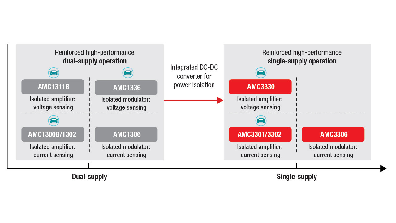
 Figure 2 TI’s portfolio of isolated amplifiers and modulators (ADCs)
Below are all of the options in the AMC3301 family, based on the application.
For current sensing:
- AMC3301: ±250-mV input reinforced isolated amplifier.
- AMC3301-Q1: Automotive Electronics Council (AEC)-Q100-qualified ±250-mV input reinforced isolated amplifier.
- AMC3302: ±50-mV input reinforced isolated amplifier.
- AMC3306M25: ±250-mV input reinforced isolated modulator (ADC).
For voltage sensing:
- AMC3330: ±1-V input reinforced isolated amplifier.
- AMC3330-Q1: AEC-Q100-qualified ±1-V input reinforced isolated amplifier.
It is possible to have both a simplified design and a compact form factor without compromising performance. When you are ready to start designing, TI’s applications experts are here to answer any questions you may have in the TI E2E™ support forums. In the meantime, check out the additional resources below to boost your knowledge on isolated amplifiers and ADCs.
Additional resources
- Learn more about isolated amplifiers and modulators in our video training series.
- Read these white papers:
- Read the application brief, Accuracy Comparison of Isolated Shunt and Closed-Loop Current Sensing.