SSZTB57 June 2016 CSD17570Q5B , CSD17573Q5B , CSD17576Q5B , DRV8305
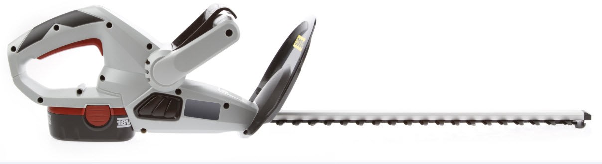
Many applications use low voltage battery (2-10 cell lithium-ion) powered motor drives like power tools, garden tools and vacuum cleaners. These tools use brushed or brushless DC motors (BLDC). BLDC motors are more efficient and have less maintenance, low noise and longer life spans.
The most important performance requirements of the power stage required to drive these tools are small form factor, high efficiency, better thermal performance, reliable protection and peak-current capability. The small form factor of the power stage enables flexible mounting, better board layout performance and low-cost designs. High efficiency provides maximum battery life and reduces cooling efforts.
To obtain higher efficiency, it is important to analyze the losses in a power stage and find a way to reduce the total losses. The main contributor of losses in an inverter comes from the MOSFETs.
In battery-powered motor-drive applications like power tools, garden tools and vacuum cleaners, the MOSFET conduction losses are responsible for approximately 60-80% of the total inverter loss. The conduction losses in a MOSFET depend on the on-state resistance (RDS_ON) of the FET and the RMS (Root Mean Square) current through the FET, calculated using Equation 1:
(1) where I RMS is the MOSFET's RMS current.
To reduce the conduction losses, select a MOSFET with minimum RDS_ON. TI’s CSD17576Q5B (RDS_ON = 2mΩ), CSD17573Q5B (RDS_ON = 1mΩ) and CSD17570Q5B (RDS_ON = 0.69mΩ) are 30V, 5mm-by-6mm SMD MOSFETs with very low RDS_ON, which can help you design a high-efficiency power stage.
Selecting a MOSFET with a minimum RDS_ON isn’t going to reduce conduction losses completely, however. The gate driver also has a role in determining MOSFET conduction losses. Let’s look at how.
The RDS_ON of the FET is not a constant but depends mainly on two factors:
- The available gate-to-source voltage (VGS) of the MOSFET.
- The MOSFET case temperature.
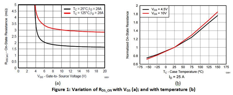
Figure 1 shows the variation of RDS_ON of a typical MOSFET (the CSD17576Q5B) with VGS and temperature.
To operate the MOSFET at the minimum RDS_ON:
- The MOSFET case temperature should be as low as possible. You can achieve this through better cooling efforts: increasing the PCB area, connecting a heat sink or providing forced airflow. All of these efforts require extra cost, however.
- Drive the FET with maximum VGS (within the FET’s maximum VGS rating) using an efficient and smart gate driver.
If you look at the RDS_ON versus VGS curve, the minimum RDS_ON occurs at a VGS of 20V. For most power FETs, the absolute maximum VGS rating is 20V and should provide good design margin in VGS for reliable operation of the MOSFET and system. Further from Figure 1(a), you can see that from 10V to 20V, the variation in RDS_ON is reasonably small. So if you consider a safety margin on the VGS, any gate-drive voltage from 10V to 15V should be good enough to drive the FET at the minimum RDS_ON. Most MOSFET gate drivers come with a gate-drive voltage output from 10V-15V and are available in different topology configurations like low or high side, half bridge, full bridge, or three phase.
Non-isolated gate drivers derive the gate-drive voltage from the battery-supply voltage using an integrated or external linear or switching regulator. In some gate drivers, as the battery DC voltage falls the gate-drive voltage also falls, depending on the available DC bus voltage.
If your application demands operation of the power stage down to a lower voltage (such as 5V in the case of a two-cell lithium-ion battery), normal gate drivers can only provide 5V or less at gate to source; the MOSFETs will be conducting at a high RDS_ON. This reduces the power-stage efficiency drastically at low DC bus voltages. Thus, you may prefer a gate driver with a higher gate-drive voltage even at lower DC bus voltages.
Let’s see how the DRV8305 three-phase gate driver from Texas Instruments can help you.
The DRV8305 is a three phase gate driver operating from 4.5V to 45V with internal charge pump supporting 100% duty cycle. The device can support low voltage applications like power tools operating from 2-cell lithium-ion battery. The DRV8305 uses a triple-charge pump to generate the proper gate-to-source voltage bias for high-side N-channel MOSFETs. Similar to the popular bootstrap architecture, the charge pump generates a floating supply voltage to enable the MOSFET. To support low-voltage operation, the DRV8305 a uses a regulated triple-charge pump scheme to create sufficient VGS to drive standard and logic-level high-side MOSFETs in the inverter during low-voltage transients or low DC bus voltages.
When the available DC input voltage is from 4.4V to 18V, the DRV8305’s charge pump regulates the voltage in triple mode. Beyond 18V to the maximum operating voltage, it switches over to double mode in order to improve efficiency.
The DRV8305 uses a linear regulator to generate the proper gate-to-source voltage for low-side N-channel MOSFETs. The linear regulator generates a fixed 10V supply voltage with respect to GND. To support low-voltage operation, the input voltage for the linear regulator is taken from the high-side charge pump. This allows the DRV8305 to provide sufficient VGS to drive standard and logic-level MOSFETs during the low-voltage transient.
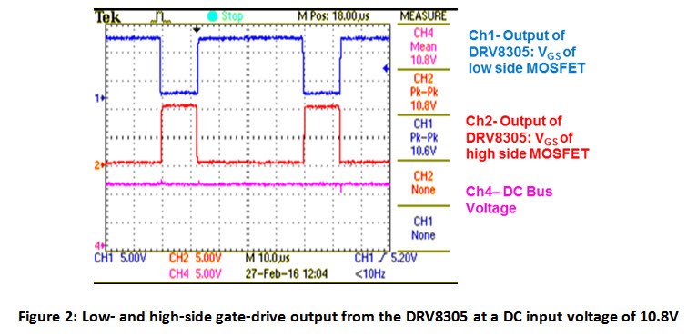
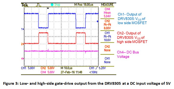
Figures 2 and 3 show test results from the 10.8V/250W 97% Efficient, Compact Brushless DC Motor Drive with Stall Current Limit reference design (TIDA-00771) showing the gate-driver output waveforms. Figure 2 shows the gate-drive output waveforms when the input DC supply voltage is 10.8V. The low- and high-side gate-drive output voltage is approximately 10V, which drives the inverter at its maximum efficiency.
Figures 3 shows the gate-drive output waveforms when the input DC supply voltage is 5V. The low-side gate-drive output voltage is approximately 10V and the high-side gate-drive output voltage is approximately 8V. The internal triple-charge pump of the DRV8305 ensures the availability of a higher gate-drive output voltage. From figure 1(a), it can be observed that the RDS_ON decreases by 25-30% when the available VGS increase from 4.5V to 8V. This means, with the triple charge pump feature of DRV8305, the MOSFET conduction loss can be reduced by 25-30% at lower DC bus voltage (5V) and hence higher efficiency.
To reduce conduction losses, you must select both a MOSFET with the lowest RDS_ON and a proper gate driver that can provide the maximum gate-drive voltage for all available input DC voltages.
Additional Resources
- Check out the complete list of MOSFETs at different voltage levels.
- View more solutions to enable your motor-control designs.
- View more solutions on motor drive power stage designs for cordless power tools
- To learn about the fundamentals of BLDC motor control, read the application report, “Sensorless Trapezoidal Control of BLDC Motors.”