SWRA760A April 2023 – April 2024 AWR2544 , AWR2944
2 Introduction
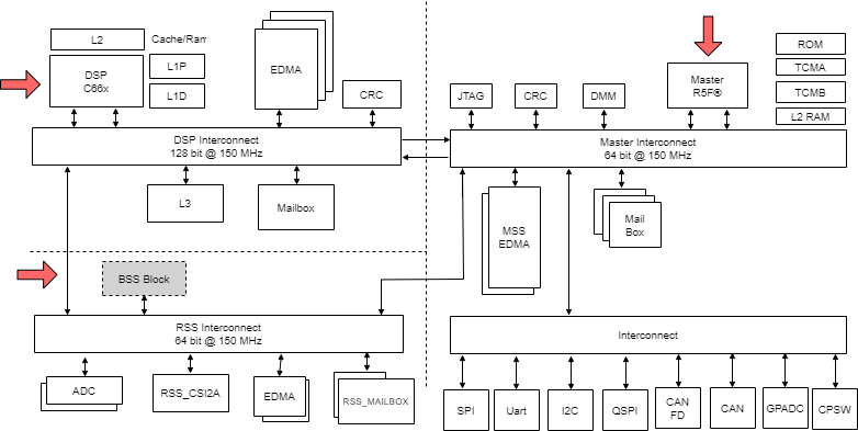
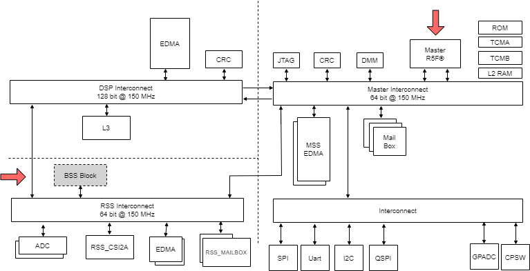
The AWR294x/AWR2544 device can be broadly split into three subsystems (see Figure 2-1,Figure 2-2), as follows:
- Main subsystem (MSS): ARM® Cortex®-R5F and associated peripherals, hosts the user application
- DSP subsystem (DSS): TI C66x and associated peripherals, hosts the user application. The DSP core TI C66x is not applicable for AWR2544 as the core is not there in the design.
- Radar/BIST SubSystem: Programmed using predefined message transactions specified by TI (reference driver : mmWaveLink provided by TI). This subsystem is black box and not available for user application.
 Figure 2-1 AWR294x Subsystems
 Figure 2-2 AWR2544 Subsystems
User application components (R5F and DSP) are expected to be stored in the serial data flash (SDF) interfaced to the AWR294x device over the quad serial peripheral interface (QSPI) interface. For AWR2544 user application component is R5F appimage only as the DSP is not applicable.
Main subsystem is the first programmable block to get activated after the AWR294x/AWR2544 device reset is de-asserted. The bootloader of the AWR294x/AWR2544 device is hosted in the read-only memory (ROM) of the main subsystem, and takes control immediately.
From this point onward, the AWR294x/AWR2544 bootloader can operate in two modes: flashing and functional. The bootloader checks the state of the sense on power (SOP) I/Os – SOP lines driven externally for choosing the specific mode (see Table 2-1).
| SOP2 (T17) | SOP1 (R14) | SOP0 (R14) | Bootloader Mode and Operation |
|---|---|---|---|
| 0 | 0 | 1 |
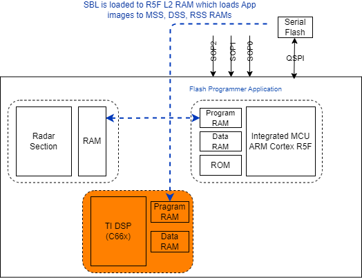
Functional or QSPI Boot Mode The RBI loads the SBL from the QSPI serial flash to the internal RAM (MSS L2) and switches the over control. |
| 1 | 0 | 1 |
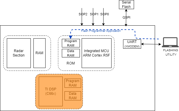
Flashing or UART Boot mode The RBL spins in loop to allow user to load SBL or the User application over UART(XMODEM) to RAM directly. This mode can be used to load the flash programmer application to RAM which further is responsible to load SBL and user application to SFLASH. |
UART boot mode of the RBL allows an external entity to load the customer application (Flash programmer) image to the RAM (MSS L2 only) which further downloads Secondary Bootloader (SBL) and/or user application to SDF (see Figure 2-3 ).
 Figure 2-3 Flashing Mode of RBL
Functional mode of the RBL relocates the image stored in the SDF to the R5F memory subsystems, this R5F image is SBL. Towards the end of this process, the bootloader passes control to R5F user defined SBL. Loading and unhaulting (start execution) of the DSP and R4F (BSS) image/core is the responsibility of the SBL (see Figure 2-4).
 Figure 2-4 Functional Mode of RBL
Key points
- AWR294x’s RBL can load only one primary user image (can have content for R5F L2 only).
- This primary user image is SBL which takes responsibility to load & download MSS, DSS and BSS image/patch to/from SDF. Customer must invest in SBL to handle multiple images (factory programmed, back-up, and so on).