SCEA122 January 2023 LSF0102 , SN74LXC1T45 , SN74LXC2T45 , SN74LXC8T245 , TXS0102 , TXS0104E , TXU0101 , TXU0102 , TXU0104 , TXU0204 , TXU0304
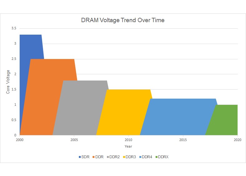
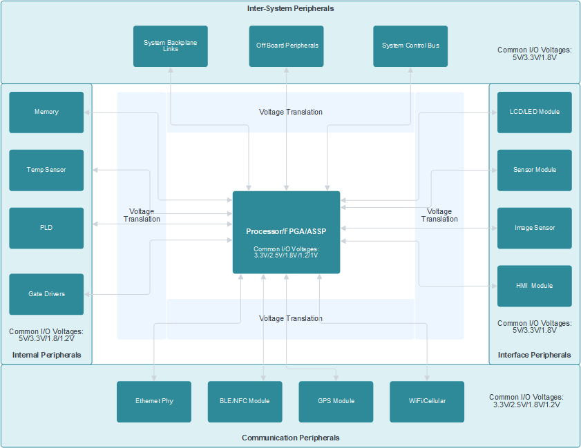
Electronic system designs in market sectors ranging from Industrial, Communications, Enterprise, Personal Electronics, and Automotive are all becoming smarter, more power efficient, and more interconnected. These market trends in electronic systems are driving system designers to adopt the latest processing technologies in terms of microprocessors, FPGAs, and Application Specific Processors (ASSP) that incorporate more functionality and operate at much lower power levels. New processor technologies are being developed using extremely small silicon processes geometries that are driving processor core voltages much lower than traditional voltage levels that are often found on peripheral devices such as sensors, optical transceivers, and HMI modules just to name a few. Selecting all the devices in a system to operate with the same I/O voltage is virtually impossible especially for larger systems. The dramatic reduction in core voltage levels of processor technologies has followed the same silicon process arc as memory devices over the past twenty years. As shown in the graph one below, memory has transitioned from 3.3 V Vdd when SDR (Single Data Rate) was the prominent memory interface standard to approximately 1 V Vdd level with today’s DDR4 (Double Data Rate) and DDR5 memory interfaces. The movement of highly integrated processor and memory devices to core voltages below common voltage rails such as 3.3 V and 1.8 V has also resulted in the I/O voltage these devices can support to scale downward. The reduction in the I/O voltage that new low power processors, ASSP, and FPGA devices can support has resulted in design challenges for system designers as they try to interconnect these processors with peripheral devices that need to operate at higher I/O voltage levels. System designers need to select peripheral devices based on parameters not related to I/O voltage such as data rate, sensitivity, and drive strength to name a few. The I/O level mismatch between lower power processors and peripheral devices often spans multiple interface types and signaling standards. Interfaces such as I2C, SPI, MDIO, RGMII, SMBus, I2S, GPIO and many others often need to be level shifted between processors and peripheral devices. System designers are turning to integrated level shifter IC devices to help resolve I/O level mismatches between devices in their designs in an easy, efficient, and cost-effective manner without having to sacrifice system performance. See figure one below for common system peripherals that may need level translation based on how the systems processor I/O is provisioned. Level shifting devices are available in a wide variety of voltage level ranges, channel configurations, and I/O types. Texas Instruments offers a large portfolio of level translation solutions that are capable of addressing level translation needs for most processor to peripheral interconnects. The Texas Instruments level translation portfolio consists of direction controlled, auto-bidirectional, fixed direction and application specific level translation devices supporting push-pull and open-drain I/O types. Selecting a level translation device for use with processors or FPGAs will depend on factors such as I/O resources available, control interfaces used, and I/O types that are provisioned within the FPGA or processor. Key considerations for system designers when selecting a level translator device includes voltage levels needing translation, number of bits or channels that need to be converted, current drive needed, data rate and directionality. For common interface types such as SPI, UART and JTAG, push-pull level translation devices from TI’s SN74AXC, SN74LXC, TXU and TXB families can provide solutions that are easy to implement with industry standard footprints. For open drain interfaces like I2C, SMBus, and MDIO, TI’s TXS, and LSF level translation families provide cost effective solutions that are available in a wide variety of channel counts and industry standard package types. For a list of recommended level translation devices for common interface types please see table one. For more information on all of TI’s level translation solutions please visit TI’s level translation landing page.
 Figure 1-1 DDR Memory Voltage Trend Over Time
 Figure 1-2 Potential System Peripherals and Sub-Systems Requiring Level Translation
| Translation Level | ||
|---|---|---|
| Interface | Up to 3.6 V | Up to 5.5 V |
| FET Replacement | 2N7001T | SN74LXC1T45 / TXU0101 |
| 1 Bit GPIO/Clock Signal | SN74AXC1T45 | SN74LXC1T45 / TXU0101 |
| 2 Bit GPIO | SN74AXC2T245 | SN74LXC2T45 / TXU0102 |
| 2-Pin JTAG/UART | SN74AXC2T45 | SN74LXC2T45 / TXU0202 |
| I2C/MDIO/SMBus | TXS0102 / LSF0102 | TXS0102 / LSF0102 |
| IC-USB | SN74AVC2T872 / TXS0202 | NA |
| 4 Bit GPIO | SN74AXC4T245 | TXB0104 / TXU0104 |
| UART | SN74AXC4T245 | TXB0104 / TXU0204 |
| SPI | SN74AXC4T774 / TXB0104 | TXB0104 / TXU0304 |
| JTAG | SN74AXC4T774 / TXB0104 | TXB0104 / TXU0304 |
| I2S/PCM | SN74AXC4T774 / TXB0104 | TXB0104 / TXU0204 |
| Quad-SPI | TXB0106 | TXB0106 |
| SDIO/SD/MMC | TXS0206 / TWL1200 | NA |
| 8 Bit GPIO/RGMII | SN74AXC8T245 | SN74LXC8T245 |