SLUAAM1 August 2022 LM5113 , LM5113-Q1 , LMG1020 , LMG1025-Q1 , LMG1205 , LMG1210 , UCC27611
GaN FET Benefits Over Silicon
Gallium Nitride FETs are now providing designers and customers with a practical and viable alternative to Silicon MOSFETs in higher density applications. GaN devices operate faster with high speed switching in the Mega Hertz range. GaN devices are also smaller, allowing high power density systems. Additionally, GaN devices are more efficient with lower switching energy and reverse recovery losses.
Nomenclature of GaN FETs
GaN FET nomenclature is very similar to that of Si MOSFETs. Similar to Si MOSFETs, GaN FETs also have a Gate, Source and Drain terminal. However, GaN power switches do not have a body diode as Si MOSFETs do.
Types of GaN FETs
Currently, the major commercial GaN FETs are lateral high-electron-mobility transistors (HEMTs). These GaN switching devices come in two different types: enhancement mode (e-GaN) and depletion mode (d-GaN).
An enhancement mode transistor is normally off and is turned on by positive voltage applied at the gate.
A depletion mode transistor is normally on and requires the use of negative voltage applied at the gate to turn off.
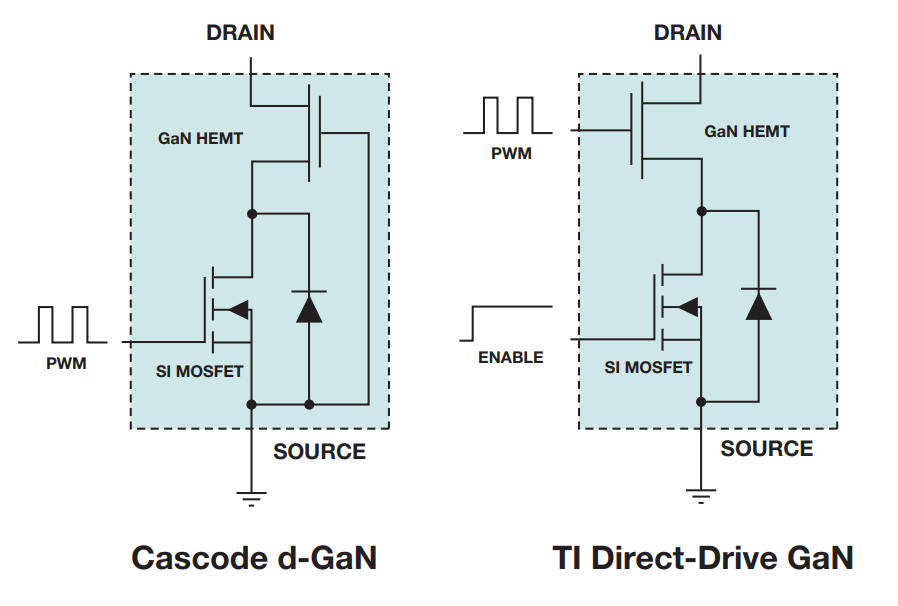
To allow normally off operation of a depletion mode GaN HEMT, it can be packaged in cascode with a low voltage Silicon switch as shown in Figure 1-1. The GaN FET is turned on or off by switching the Si FET on or off in every cycle.
TI’s solution is to have the GaN FET driven directly as shown in Figure 1-1, where the Silicon switch is used as an enable switch at start-up, so the Si switch does not switch in every cycle, only the GaN switch does.
 Figure 1-1 Configuration Difference Between Cascode d-GaN and Direct-Drive GaN
GaN FET Structure
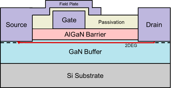
Figure 1-2 shows a basic example of a lateral structure of GaN FETs. In this structure, we have the silicon substrate, gallium nitride buffer, aluminum gallium nitride barrier, our three terminals: source, gate and drain, a layer of passivisation (protection dielectric) and a field plate extending from the source terminal.
GaN HEMTs require a passivisation layer to reduce the effects of surface electron traps between the gate and drain contacts. The benefits of the field plate are an increase of the breakdown voltage and a reduction of the surface electron traps.
The hetero junction of the AlGaN barrier and GaN buffer – which is a type of junction between two different semiconductors – forms a 2-dementional electron gas channel (2DEG). This channel has very high charge density and mobility. Current flows in the 2DEG channel versus in a Si MOSFET where the channel for current flow is the depletion region between the source and drain.
 Figure 1-2 Basic Lateral Structure of a GaN FET
No Body Diode
Previously, we mentioned that GaN FETs have no body diode. The body diode in Si MOSFETs forms from the pn junction between the source and drain. However, we do not have this junction in GaN FETs and that is why there is no body diode.