SBAA507 March 2021 ADS8578S , ADS8584S , ADS8586S , ADS8588H , ADS8588S , ADS8598H , ADS8598S , ADS8661 , ADS8664 , ADS8665 , ADS8668 , ADS8671 , ADS8674 , ADS8675 , ADS8678 , ADS8681 , ADS8684 , ADS8684A , ADS8685 , ADS8688 , ADS8688A , ADS8688AT , ADS8689 , ADS8691 , ADS8694 , ADS8695 , ADS8698 , ADS8699 , OPA2990 , OPA4990 , OPA990
DC Transfer Characteristics
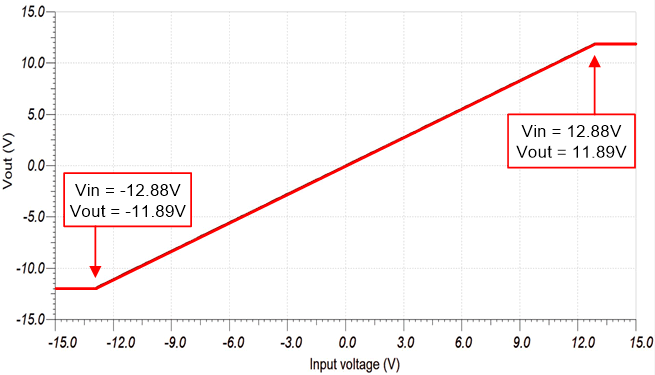
The following graph shows a linear output response of the front-end circuit for input from single-ended –12.88V to +12.88V. See Determining a SAR ADC’s Linear Range when using Instrumentation Amplifiers for detailed theory on this subject. The full-scale range (FSR) of the ADC falls within the linear range of the amplifier (OPA990).