SBAU251B July 2017 – February 2023
5.1 Default Jumper Settings
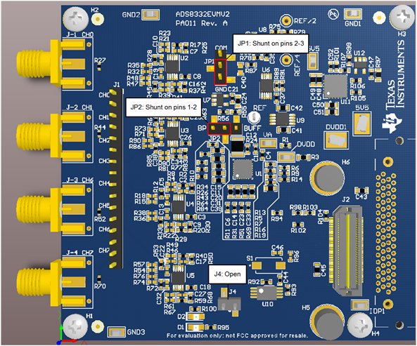
Make sure jumpers JP1, JP2, and J4 are in the default configuration while interfacing the ADS8332EVMV2 board with the PHI controller as described in Table 5-1. The jumpers can be reconfigured to allow for different types of operation.
Figure 5-1 details the default jumper settings.Table 5-1 explains the configuration for these jumpers.
 Figure 5-1 ADS8332EVMV2 Default Jumper Settings
Table 5-1 Default Jumper Configuration
| Jumper | Function | Default Position | Description | ||
|---|---|---|---|---|---|
| JP1 | Common pin voltage | Shunt on pins 2-3 | Shunt on pins 2-3 select ground as the common pin voltage | ||
| JP2 | Multiplexer output buffer | Shunt on pins 1-2 | Shunt on pins 1-2 selects to bypass the buffer between MUXOUT and ADCIN | ||
| J4 | EEPROM write enable | Open | Open enables write protect for the EEPROM | ||