SBAU269C October 2016 – August 2021 ADS8900B
5.3 Default Jumpers for Bipolar, Single-Ended Inputs
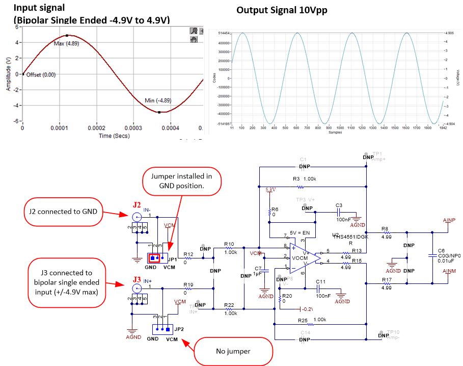
The EVM can be jumper configured for both differential and single-ended inputs. The jumpers also impact the common-mode (offset) requirements for the input signal. Some jumpers are only used in unusual circumstances, and are normally configured as described in this section. Table 5-2 provides jumper configurations for a bipolar, single-ended input. Figure 5-6 shows the input full-scale signal and the ADC output. The output signal is half full scale.
Table 5-2 Jumper Configurations for
Bipolar, Single-Ended Input
| Jumper | Default Setting | Purpose |
|---|---|---|
| JP1 | GND position | When installed in this position, the input J2 is connected to GND. Connect the input J3 to a single-ended input signal with the offset set to 0 V (bipolar input). |
| JP2 | Removed | Leave this jumper unconnected, and apply a single-ended signal with a 0-V offset to connector J3. |
| JP3 | 2.6-V position | Both the 2.5-V and 2.6-V position can be used for a fully differential input signal. The 2.6-V position shifts the signal from GND by 0.1 V to minimize distortion resulting from output swing limitations. This shift works because the amplifier positive supply is set to 5.3 V. The signal out of AINP and AINN ranges from 0.1 V to 5.1 V when the jumper is in the 2.6-V position. The signal out of AINP and AINN ranges from 0 V to 5.0 V when the jumper is in the 2.5-V position. |
| JP4 | GND position | This jumper selects the negative supply voltage. The default board configuration does not include the negative supply, so the –0.2-V position does not work without installing U6 and the associated components. |
| JP5 | Removed | Removing this jumper sets the EEPROM write protect on. The EEPROM is factory programed and does not need to be reprogrammed, so keeping the write protect on is recommended. |
 Figure 5-6 Bipolar, Single-Ended, –5.0-V to 5.0-V
Input