SBAU394A April 2022 – September 2022
- ADS1285 Evaluation Module
- Trademarks
- 1 EVM Overview
- 2 ADS1285EVM-PDK Quick-Start Guide
- 3 EVM Analog Interface
- 4 Digital Interface
- 5 Power Supplies
- 6 Digital-to-Analog Converter
- 7 ADS1285EVM-PDK Initial Setup
- 8 ADS1285EVM-PDK Software Reference
- 9 ADS1285EVM-PDK Bill of Materials, PCB Layout, and Schematics
- 10References
- 11Revision History
9.3 Schematics
Figure 9-7 shows a block diagram of the ADS1285EVM-PDK.
Figure 9-7 ADS1285EVM-PDK Block Diagram
Figure 9-8 through Figure 9-13 illustrate various schematics for the ADS1285EVM-PDK ADC.
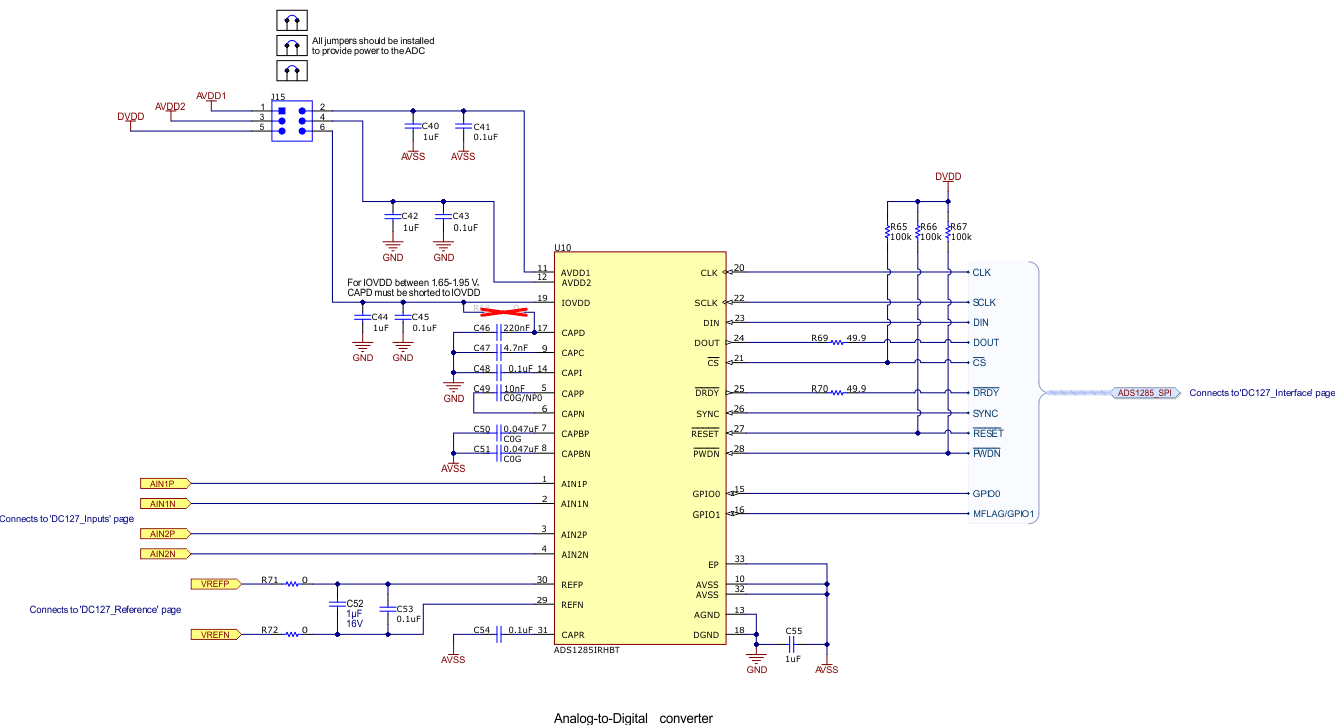 Figure 9-8 ADS1285EVM-PDK ADC Schematic
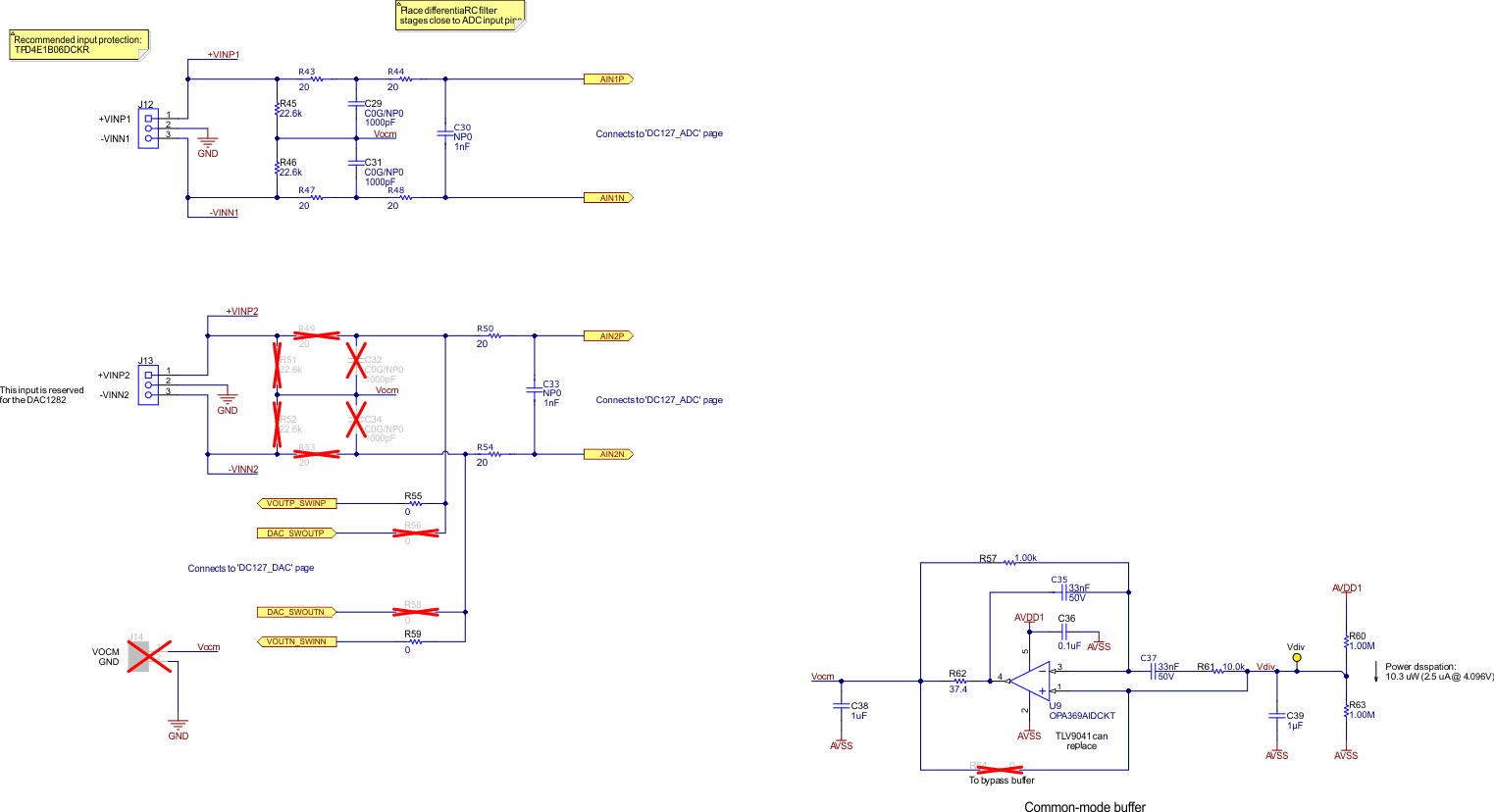 Figure 9-9 ADS1285EVM-PDK Analog Inputs and Common-Mode Buffer Schematic
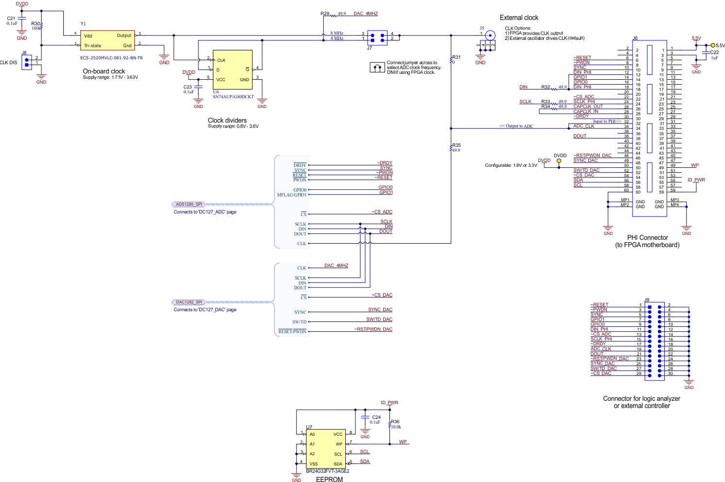 Figure 9-10 ADS1285EVM-PDK Clock and Interface Schematic
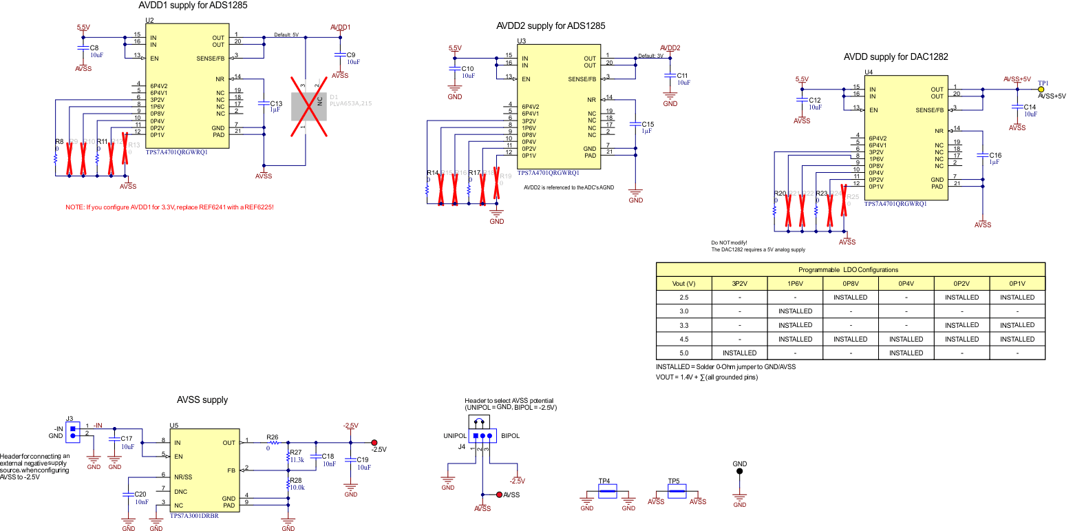 Figure 9-11 ADS1285EVM-PDK Power-Supply Schematic
 Figure 9-12 ADS1285EVM-PDK Reference Voltage Schematic
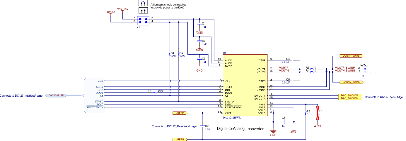 Figure 9-13 ADS1285EVM DAC Schematic