SBAU394A April 2022 – September 2022
- ADS1285 Evaluation Module
- Trademarks
- 1 EVM Overview
- 2 ADS1285EVM-PDK Quick-Start Guide
- 3 EVM Analog Interface
- 4 Digital Interface
- 5 Power Supplies
- 6 Digital-to-Analog Converter
- 7 ADS1285EVM-PDK Initial Setup
- 8 ADS1285EVM-PDK Software Reference
- 9 ADS1285EVM-PDK Bill of Materials, PCB Layout, and Schematics
- 10References
- 11Revision History
8.1 EVM GUI Global Settings for ADC Control
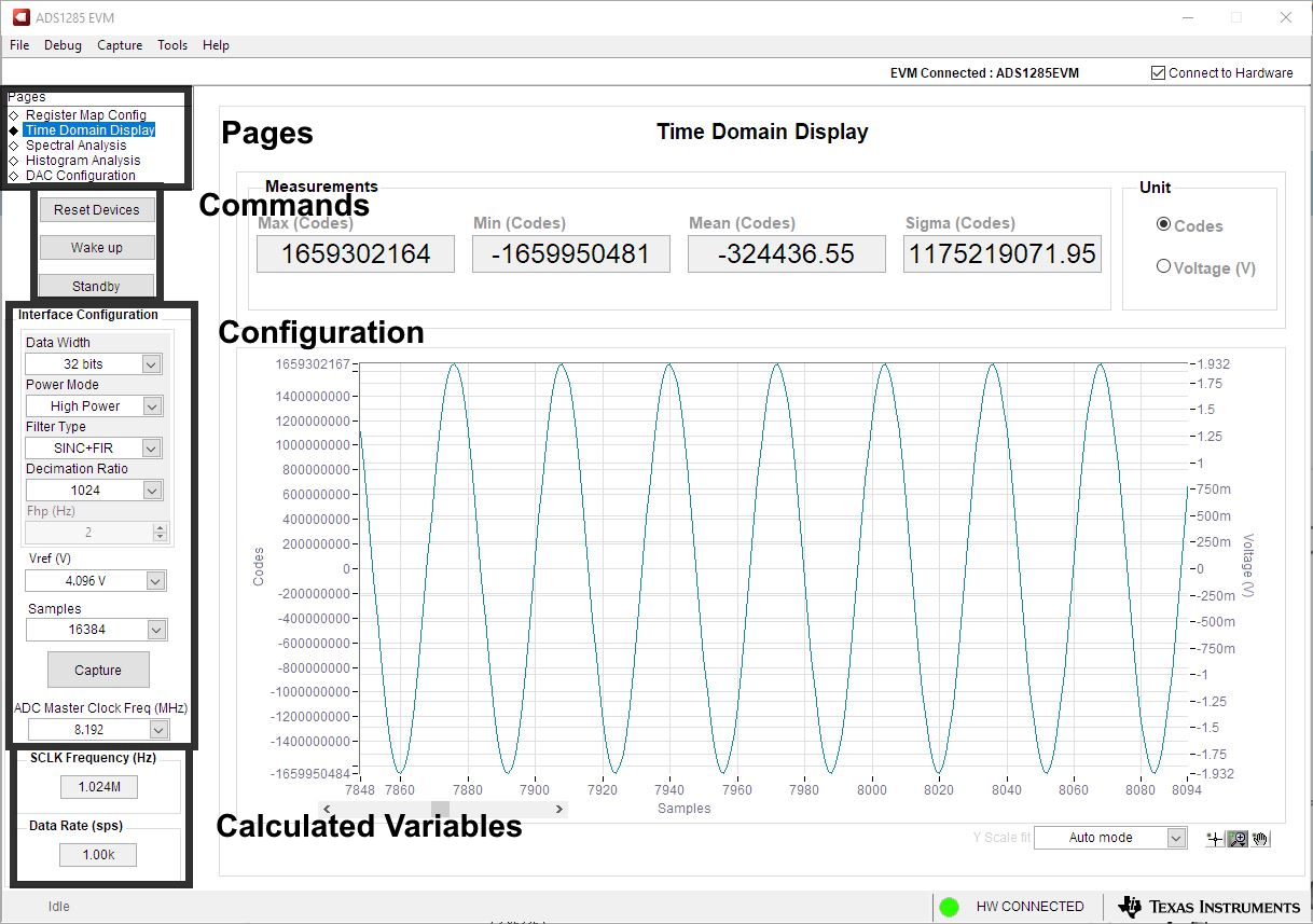
Although the EVM GUI does not allow direct access to the levels and timing configuration of the ADC digital interface, the EVM GUI does give users high-level control over many other functions of the ADS1285, including: internal clock dividers, oversampling ratio (OSR), and number of samples to be captured. Figure 8-1 identifies the input parameters of the GUI (as well as their default values) through which the various functions of the ADS1285 can be exercised.
 Figure 8-1 EVM GUI Global Input Parameters
There are four pages available in the ADS1285EVM-PDK GUI. The information area displays the results of each of the pages. Each of these pages display a different control or measurement of the device. The Register Map Config page reads and writes the registers of the device. The Time Domain Display page collects a set of data from the device and displays the result. The Spectral Analysis page can compute the FFT of the collected data, and the Histogram Analysis page shows a histogram of the collected data and displays basic statistics of the result.
The Single Commands section allows for direct control of the device for three basic functions. First, the Reset button sends a signal to the RESET pin to reset the device. The Standby button puts the device into a low-power state where all channels are disabled, and the reference and other non-essential circuitry are powered down. The Wakeup button exits standby mode.
The Interface Configuration section also sets the data rate by setting the internal clock dividers and OSR in the ADC. Finally, this section can set the power modes in the registers. The ADS1285 has three power modes (low-power, mid-power, and high-power) that are configured in the CONFIG0 register (bits 7-6). This configuration is used in conjunction with the jumper settings of JP8 for the CLK pin, as outlined in Section 3.2.
The Clock and Sampling Rate section allows the user to specify a target SCLK frequency (in Hz) and the GUI tries to match this frequency as closely as possible by changing the PHI PLL settings, but the achievable frequency may differ from the target value entered. This section also displays the sampling rate of the ADC as controlled by the internal clock dividers and the OSR.
The GUI is switched between hardware mode and simulation mode by checking and unchecking the Connected to Hardware box in the top right area of the screen at any time.