SBOA510 March 2021 OPA455 , OPA462
- Trademarks
- 1Introduction
- 2Three Op Amp OPA462 HV Solution
- 3Lower Voltage, Lower Cost Three Op Amp Solution
- 4OPA462 300 Vpp Output Solution With Discrete Transistor Supply-Rail Drivers
- 5Lessons Learned from the Practical Implementation of the HV Op Amp Solutions
-
A Appendix
- A.1 Overview
- A.2 Summary of Results
- A.3 Test Setup and Equipment
- A.4 Printed Circuit Boards
- A.5 Power Supply, Source Measurement Unit (SMU)
- A.6 Arbitrary Waveform Generator (AWG)
- A.7 Oscilloscope
- A.8 Circuit 1: OPA462 Three op amp Solution
- A.9 Circuit 2: Lower Voltage, Lower Cost Three Op Amp Solution
- A.10 Circuit 3: OPA462 300 Vpp Output Solution With Discrete Transistor Supply-Rail Drivers
2 Three Op Amp OPA462 HV Solution
Suppose an HV op-amp application requires a 300-Vpp output voltage to be developed across its output load. That output voltage is much higher than the absolute maximum supply capabilities of the OPA454 ±60 V (120 V) and OPA462 ±95 V (190 V) listed in their data sheets. Note that relative to ground, the supply magnitudes of an op amp can be higher than the rated maximums provided the voltage across its power supply pins does not exceed the absolute maximum voltage rating. For example, an OPA462 could be safely operated with V+ = +280 V and V– = +100 V, as the voltage across the supply pins would be 180 V. If this kind of supply arrangement is used, the input and output conditions must remain within the linear operating regions relative to the HV levels applied to the supply pins. The input of the amplifier circuit could not be grounded, for example, as this would appear to the op amp as an input signal 100 V below the low rail, far outside the safe operating region.
There are techniques applied in linear circuits that are used to enhance a particular performance characteristic of an amplifier. The techniques tap into a voltage, or current often obtained from the output stage, and then uses it to enhance the performance of an earlier stage in the amplifier. For example, one might access an output stage electrical property to effectively increase the impedance seen at the amplifier input. This technique is often referred to as bootstrapping. Bootstrapping will not be used to alter the general electrical characteristics of the OPA462 HV op amp, but instead applied here to increase the output voltage range of an OPA462 circuit so that it is able to provide the stated 300 Vpp across the output load.
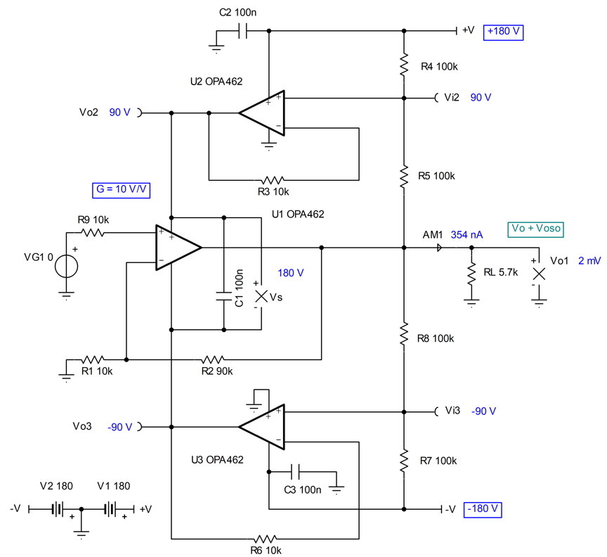
Figure 2-1 shows a circuit solution that increases the output voltage swing range to 300 Vpp and is composed of three OPA462 HV op amps.
 Figure 2-1 Three OPA462 Op Amp HV
Solution
Figure 2-1 Three OPA462 Op Amp HV
SolutionOp amp U1, an OPA462 HV op amp, is the signal path amplifier amplifying the input signal provided by signal source VG1. It is set up in this case for a non-inverting gain of +10 V/V. Its closed-loop gain is established from the simple relationship, Av = 1 + (R2 / R1). A 30 Vpp input at VG1 results in a 300 Vpp output voltage being developed across RL. Although the 300 Vpp exceeds the OPA462 absolute maximum supply rating of 190 V, the other two OPA462 op amps U2 and U3 control the supply voltages of U1, keeping them safe and within the maximum rating.
The output pins of the other two OPA462 op amps, U2 and U3, actively drive the V+ and V– supply pins of the U1, and supply its operating current IQ and the load current it delivers to RL. Each is connected as a voltage follower having a gain of + 1 V/V. Resistive voltage dividers R4, R5 and R7, R8, connected between their associated +V or –V supply line, and the U1 output voltage at any moment establishes the U2 and U3 input voltages. Since the resistors of each divider are equal in the corresponding non-inverting input voltage will be one-half the difference between the HV supply level minus Vo1, divided by two. The voltages developed at the respective U2 and U3 non-inverting input is replicated at each of their outputs.
Shown in Figure 2-1 are the DC voltages occurring at various nodes for the three-op amp circuit. The input applied to U1 is 0 V and the +V and –V supplies are set to ±180 V for this case. The Vo1 output is nearly 0 V, deviating by the output referred voltage offset (Voso) generated by U1 in a gain of +10 V/V. The difference between the +180-V and –180-V power supplies and the U1 output at 0 V, divided by 2 via the resistive dividers, establishes the input of U1 (Vi2) at +90 V and the input at U3 (Vi3) to –90 V. This yields Vo2 at +90 V and Vo3 at –90 V, or +180 V between them. That is the voltage that appears across the supply pins of U1.
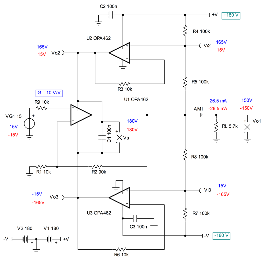
In Figure 2-2 the DC input voltage to U1 is first set to +15 V, and then set to –15 V. The node voltages shown in blue correspond to a +15-V input, while the red ones correspond to a –15-V input. Observe how the Vi2, Vo2, Vi3, Vo3 move together as the U1 input voltage changes from the 0 V to –15 V, and then to +15 V. Importantly, observe how the voltage difference across the supply pins of U1 is maintained at +180 V when VG1 set to 0 V, +15 V or –15 V. Additionally, how the output voltage range now extends from +150 V to –150 V, for a 300-V change.
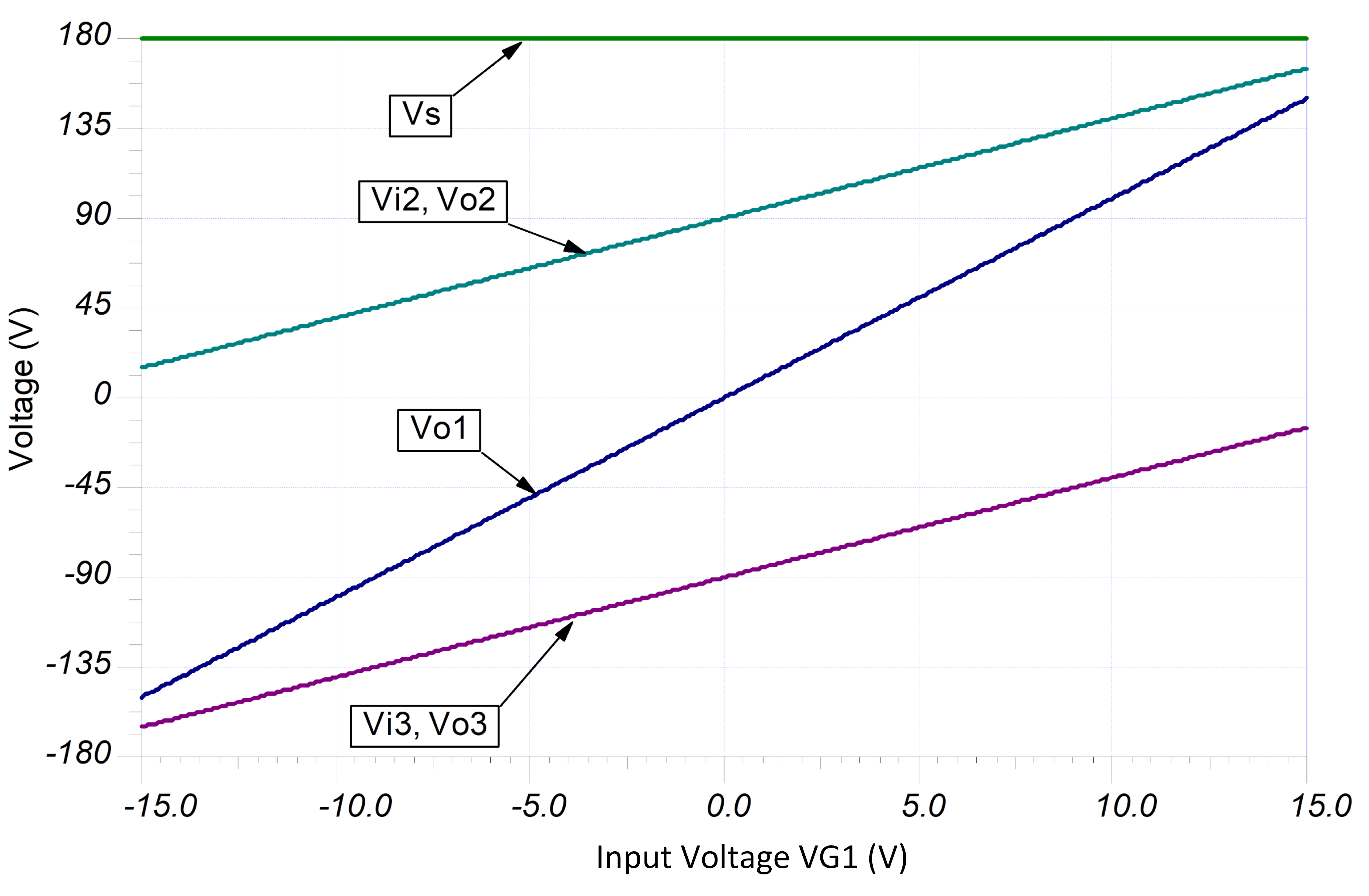
Figure 2-3 shows how the node voltages in the three OPA462 op-amp circuit change as the input voltage is swept linearly from –15 V to +15 V. The difference between the Vo2 and Vo3 voltages is equal to Vs, the voltage across the U1 supply pins. The topmost line in the graph is Vs across the input voltage range. The straight line confirms that Vs remains constant regardless of the output voltage level U1 attains at Vo1.
Noting the supply differences the electrical performances of the three OPA462 op amp HV amplifier are similar to what may be achieved by a single OPA462 operated in the same gain. The power supply rejection (PSR) capability of U1 will be more rigorously exercised because U2 and U3 can change their output voltage rapidly when following the U1 output. This is a different situation compared to when stable, regulated DC supplies are used to power the supply pins of an op amp. The OPA462 has high, power-supply rejection ratio (PSRR) of about 130 dB at DC, 80 dB at 1 kHz ,and 60 dB at 10 kHz, which helps minimize output referred voltage offset changes as the supply voltages of U1 follow its output voltage.
The OPA462 U1 power supply pin bypassing is accomplished in a manner such that U2 and U3 can tolerate the 100-nF capacitance across the U1 supply pins that they drive, without becoming unstable. The capacitor is connected between their outputs. The two op amps are connected as unity gain buffers. They provide a very low output impedance at low frequencies, and supply some of the transient current when demanded by U1. The reactance and impedance of the bypass capacitor decreases as frequency increases, being a more effective bypass at higher frequencies where the output impedance of the op amp is increasing. The combination was found to provide effective bypassing and remain stable in the lab evaluations.
 Figure 2-2 Three OPA462 HV Solution With DC
Input Voltages of +15 V (Blue) and ﹣15 V (Red)
 Figure 2-3 Circuit Voltages for the Three
OPA462 HV Solutions as the DC Input Voltage VG1 is Swept From –15 V to +15 V