SBVU066A August 2020 – April 2021 TPS51397A
5.1 Layout
The board assembly and layout for the TPS51397AEVM is shown in Figure 5-1 to Figure 5-5. The top and bottom layers are 2-oz copper thickness. Internal layers are 1-oz copper thickness.
The top layer contains the main power traces for VIN, VOUT, and ground. Also on the top layer are connections for the pins of the TPS51397A and a large area filled with ground. Most of the signal traces are located on the bottom left side, surrounded by a ground plane with an island for quiet analog ground that is connected to the main power ground at a single point. The internal layer-1 and internal layer-2 are dedicated ground planes. The bottom layer is another ground copper area with additional SW, VIN, and VOUT copper fill. Ground traces on different layers are connected to each other with multiple vias placed on the board.
The input decoupling capacitors are located as close to the IC as possible. Critical analog circuits, such as the voltage set point divider, EN resister, SS capacitor, Mode resistor, VCC, and AGND pin, are terminated to quiet analog ground island on the top layer. The input and output connectors, test points, and all of the components are located on the top side. The bottom layer is a ground plane along with the switching node copper fill, VIN and VOUT copper fill, and the feedback trace from the point of regulation to the top of the resistor divider network.
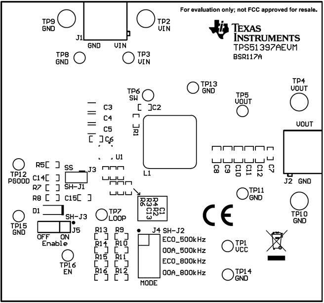 Figure 5-1 Top Assembly
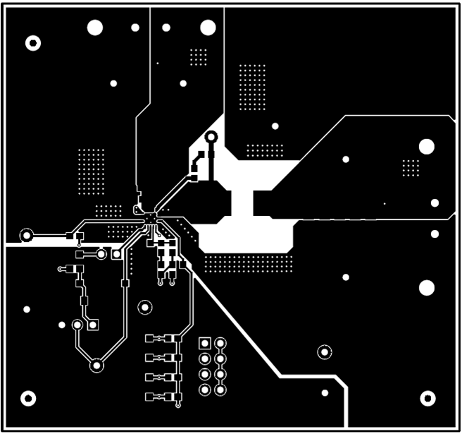 Figure 5-2 Top Layer Layout
 Figure 5-3 Internal Layer-1 Layout
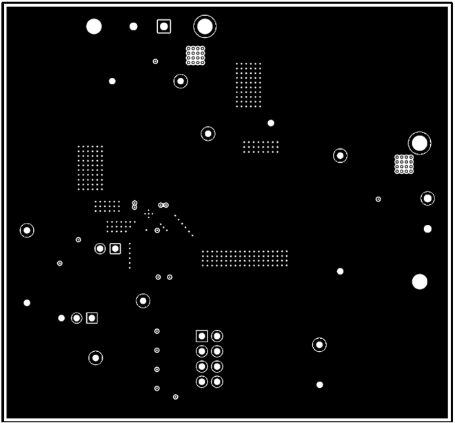 Figure 5-4 Internal Layer-2 Layout
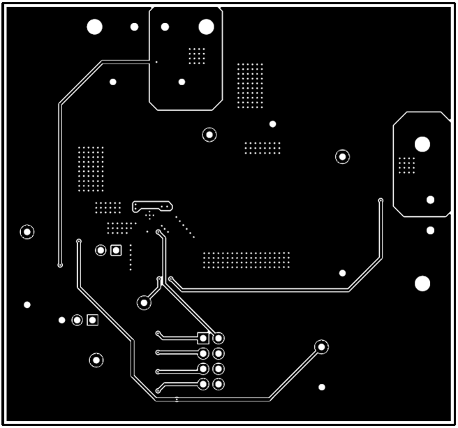 Figure 5-5 Bottom Layer Layout
The board top and bottom view for the TPS51397AEVM is shown in Figure 5-6 and Figure 5-7.
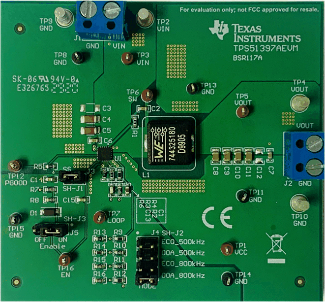 Figure 5-6 Board Top View
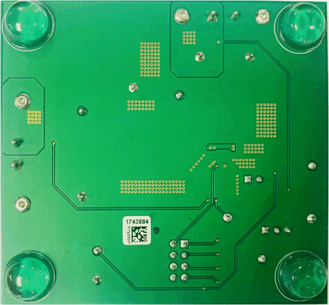 Figure 5-7 Board Bottom View