SCDS423A October   2020  – May 2024 TMUX1575

PRODUCTION DATA  

  1.   1
  2. Features
  3. Applications
  4. Description
  5. Pin Configuration and Functions
    1.     Pin Functions
  6. Specifications
    1. 5.1 Absolute Maximum Ratings
    2. 5.2 ESD Ratings
    3. 5.3 Recommended Operating Conditions
    4. 5.4 Thermal Information
    5. 5.5 Electrical Characteristics
    6. 5.6 Dynamic Characteristics
    7. 5.7 Timing Requirements
    8. 5.8 Typical Characteristics
  7. Parameter Measurement Information
    1. 6.1  On-Resistance
    2. 6.2  Off-Leakage Current
    3. 6.3  On-Leakage Current
    4. 6.4  IPOFF Leakage Current
    5. 6.5  Transition Time
    6. 6.6  tON (EN) and tOFF (EN) Time
    7. 6.7  Break-Before-Make Delay
    8. 6.8  Charge Injection
    9. 6.9  Off Isolation
    10. 6.10 Channel-to-Channel Crosstalk
    11. 6.11 Bandwidth
  8. Detailed Description
    1. 7.1 Overview
    2. 7.2 Functional Block Diagram
    3. 7.3 Feature Description
      1. 7.3.1 Bidirectional Operation
      2. 7.3.2 Beyond Supply Operation
      3. 7.3.3 1.2V Logic Compatible Inputs
      4. 7.3.4 Powered-off Protection
      5. 7.3.5 Fail-Safe Logic
      6. 7.3.6 Integrated Pull-Down Resistors
    4. 7.4 Device Functional Modes
      1. 7.4.1 Truth Tables
  9. Application and Implementation
    1. 8.1 Typical Application
      1. 8.1.1 Design Requirements
      2. 8.1.2 Detailed Design Procedure
    2. 8.2 Power Supply Recommendations
    3. 8.3 Layout
      1. 8.3.1 Layout Guidelines
      2. 8.3.2 Layout Example
  10. Device and Documentation Support
    1. 9.1 Documentation Support
      1. 9.1.1 Related Documentation
    2. 9.2 Receiving Notification of Documentation Updates
    3. 9.3 Support Resources
    4. 9.4 Trademarks
    5. 9.5 Electrostatic Discharge Caution
    6. 9.6 Glossary
  11. 10Revision History
  12. 11Mechanical, Packaging, and Orderable Information
    1. 11.1 Mechanical Data

On-Resistance

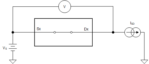
The on-resistance of a device is the ohmic resistance between the source (Sx) and drain (Dx) pins of the device. The on-resistance varies with input voltage and supply voltage. The symbol RON is used to denote on-resistance. The measurement setup used to measure RON is shown in Figure 6-1. Voltage (V) and current (ISD) are measured using this setup, and RON is computed as shown below with RON = V / ISD:
TMUX1575 On-Resistance Measurement SetupFigure 6-1 On-Resistance Measurement Setup