SCDS423A October   2020  – May 2024 TMUX1575

PRODUCTION DATA  

  1.   1
  2. Features
  3. Applications
  4. Description
  5. Pin Configuration and Functions
    1.     Pin Functions
  6. Specifications
    1. 5.1 Absolute Maximum Ratings
    2. 5.2 ESD Ratings
    3. 5.3 Recommended Operating Conditions
    4. 5.4 Thermal Information
    5. 5.5 Electrical Characteristics
    6. 5.6 Dynamic Characteristics
    7. 5.7 Timing Requirements
    8. 5.8 Typical Characteristics
  7. Parameter Measurement Information
    1. 6.1  On-Resistance
    2. 6.2  Off-Leakage Current
    3. 6.3  On-Leakage Current
    4. 6.4  IPOFF Leakage Current
    5. 6.5  Transition Time
    6. 6.6  tON (EN) and tOFF (EN) Time
    7. 6.7  Break-Before-Make Delay
    8. 6.8  Charge Injection
    9. 6.9  Off Isolation
    10. 6.10 Channel-to-Channel Crosstalk
    11. 6.11 Bandwidth
  8. Detailed Description
    1. 7.1 Overview
    2. 7.2 Functional Block Diagram
    3. 7.3 Feature Description
      1. 7.3.1 Bidirectional Operation
      2. 7.3.2 Beyond Supply Operation
      3. 7.3.3 1.2V Logic Compatible Inputs
      4. 7.3.4 Powered-off Protection
      5. 7.3.5 Fail-Safe Logic
      6. 7.3.6 Integrated Pull-Down Resistors
    4. 7.4 Device Functional Modes
      1. 7.4.1 Truth Tables
  9. Application and Implementation
    1. 8.1 Typical Application
      1. 8.1.1 Design Requirements
      2. 8.1.2 Detailed Design Procedure
    2. 8.2 Power Supply Recommendations
    3. 8.3 Layout
      1. 8.3.1 Layout Guidelines
      2. 8.3.2 Layout Example
  10. Device and Documentation Support
    1. 9.1 Documentation Support
      1. 9.1.1 Related Documentation
    2. 9.2 Receiving Notification of Documentation Updates
    3. 9.3 Support Resources
    4. 9.4 Trademarks
    5. 9.5 Electrostatic Discharge Caution
    6. 9.6 Glossary
  11. 10Revision History
  12. 11Mechanical, Packaging, and Orderable Information
    1. 11.1 Mechanical Data

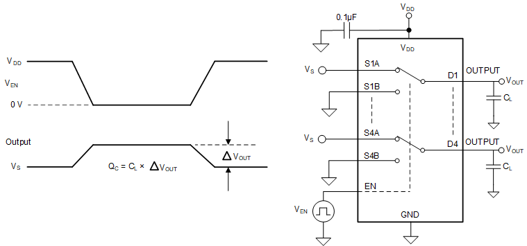
Charge Injection

The amount of charge injected into the source or drain of the device during the falling or rising edge of the gate signal is known as charge injection, and is denoted by the symbol QC. Figure 6-8 shows the setup used to measure charge injection from source (Sx) to drain (Dx).
TMUX1575 Charge-Injection Measurement SetupFigure 6-8 Charge-Injection Measurement Setup