SCEU025 May 2022
4.1 PCB Layer Stack-Up
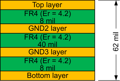
Figure 4-1 shows the CDCBT1001 printed circuit board (PCB) layer stack-up.
 Figure 4-1 PCB Layer Stack-Up
SCEU025 May 2022
Figure 4-1 shows the CDCBT1001 printed circuit board (PCB) layer stack-up.
 Figure 4-1 PCB Layer Stack-Up