SCEU025 May 2022
4.2 PCB Layout
The following figures show the CDCBT1001 printed circuit board (PCB) layout.
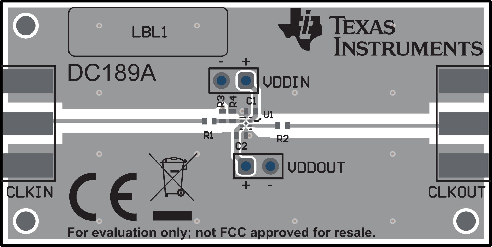 Figure 4-2 Top Layer
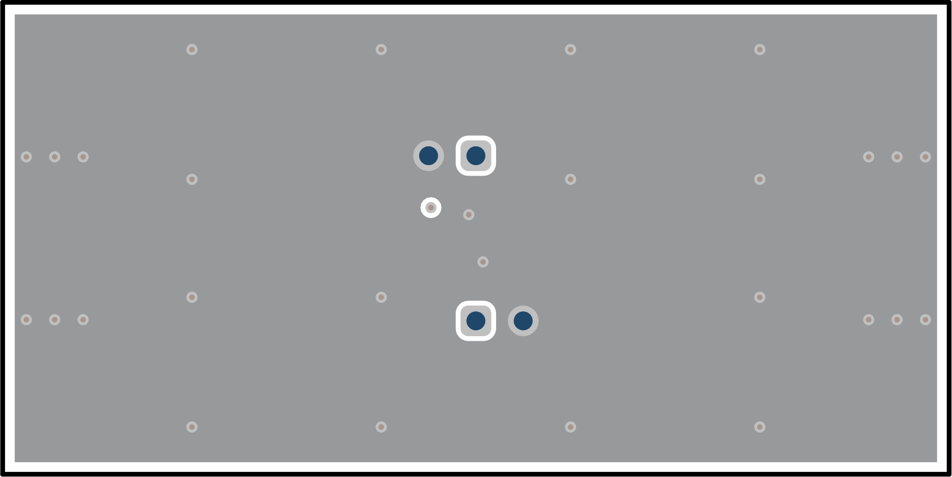 Figure 4-3 GND Layer
 Figure 4-4 GND Layer
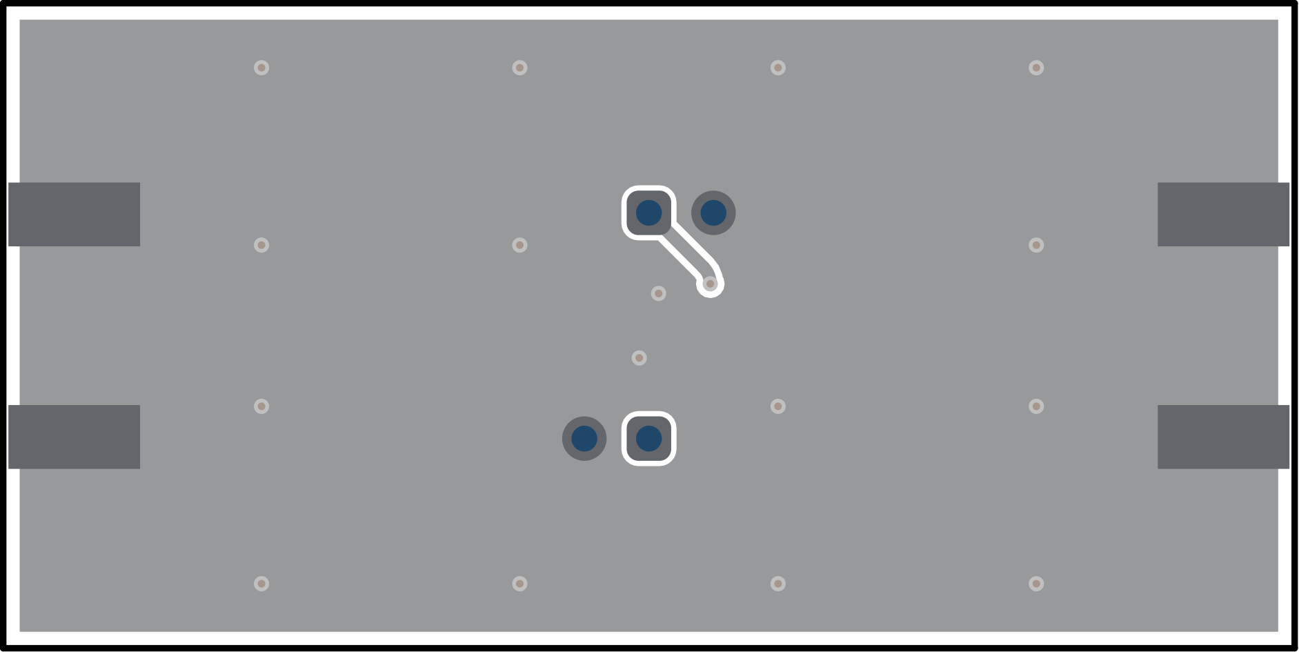 Figure 4-5 Bottom Layer
SCEU025 May 2022
The following figures show the CDCBT1001 printed circuit board (PCB) layout.
 Figure 4-2 Top Layer
 Figure 4-3 GND Layer
 Figure 4-4 GND Layer
 Figure 4-5 Bottom Layer