SFFS092 March 2021 UCC23313-Q1 , UCC23511-Q1 , UCC23513-Q1
PRODUCTION DATA
4 Pin Failure Mode Analysis (Pin FMA)
This section provides a Failure Mode Analysis (FMA) for the pins of the UCC23511-Q1, UCC23513-Q1, UCC23313-Q1. The failure modes covered in this document include the typical pin-by-pin failure scenarios:
- Pin short-circuited to Ground (see Table 4-2)
- Pin open-circuited (see Table 4-3)
- Pin short-circuited to an adjacent pin (see Table 4-4)
- Pin short-circuited to supply (see Table 4-5)
Table 4-2 through Table 4-5 also indicate how these pin conditions can affect the device as per the failure effects classification in Table 4-1.
| Class | Failure Effects |
|---|---|
| A | Potential device damage that affects functionality |
| B | No device damage, but loss of functionality |
| C | No device damage, but performance degradation |
| D | No device damage, no impact to functionality or performance |
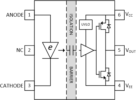
Figure 4-1 shows the UCC23511-Q1, UCC23513-Q1, UCC23313-Q1 pin diagram. For a detailed description of the device pins please refer to the Pin Configuration and Functions section in the UCC23511-Q1, UCC23513-Q1, UCC23313-Q1 data sheet.
 Figure 4-1 Pin Diagram
Following are the assumptions of use and the device configuration assumed for the pin FMA in this section:
- Pin short case No.1 to 6 and 3 to 4 are out of scope.
| Pin Name | Pin No. | Description of Potential Failure Effect(s) | Failure Effect Class |
|---|---|---|---|
| ANODE | 1 | VOUT state = L (low state). | B |
| NC (No connect) | 2 | No impact | D |
| CATHODE | 3 | Possible incorrect VOUT state. The external controller cannot control CATHODE current. | B |
| VEE | 4 | Shorting to VEE itself. No effect. | D |
| VOUT | 5 | VOUT state = L. Possible damge to device. | A |
| VCC | 6 | VOUT state = L with reduced pulled-low strength. | B |
| Pin Name | Pin No. | Description of Potential Failure Effect(s) | Failure Effect Class |
|---|---|---|---|
| ANODE | 1 | VOUT state = L (low state). VOUT does not repond to the external controller command. | B |
| NC (No connect) | 2 | No impact. | D |
| CATHODE | 3 | VOUT state = L.VOUT does not repond to the external controller command. | B |
| VEE | 4 | VOUT state = H (high state) with reduced pulled-high drive strength. VOUT does not repond to the external controller command. | B |
| VOUT | 5 | VOUT is diconnected from the system. | B |
| VCC | 6 | VOUT state = L with reduced pulled-low strength. | B |
| Pin Name | Pin No. | Shorted to | Description of Potential Failure Effect(s) | Failure Effect Class |
|---|---|---|---|---|
| ANODE | 1 | NC | No impact. | D |
| NC (No connect) | 2 | CATHODE | No impact. | D |
| CATHODE | 3 | Not Applicable | Not Applicable | Not Applicable |
| VEE | 4 | VOUT | VOUT state = L. Possible damge to device. | A |
| VOUT | 5 | VCC | VOUT state = H. Possible damge to device. | A |
| VCC | 6 | Not Applicable | Not Applicable | Not Applicable |
| Pin Name | Pin No. | Description of Potential Failure Effect(s) | Failure Effect Class |
|---|---|---|---|
| ANODE | 1 | The external controller can't command ANODE to CATHODE current via ANODE pin. | B |
| NC (No connect) | 2 | No impact. | D |
| CATHODE | 3 | VOUT state = L. VOUT does not repond to the external controller command. | B |
| VEE | 4 | VOUT state = L with reduced pulled-low drive strength | B |
| VOUT | 5 | VOUT state = H. Possible damge to device. | A |
| VCC | 6 | Shorting to VCC itself. No effect. | D |