SLAA870 February 2019 AFE7422 , AFE7444
-
Evaluating the frequency hopping capability of the AFE74xx
- Trademarks
- 1 Introduction
- 2 Phase Coherency vs Phase Continuity
- 3 AFE74xx Architecture
- 4 Frequency Hopping Methods
- 5 NCO Frequency Resolution Versus Hop Time
- 6 Fast Frequency Hopping With the Load and Switch
- 7 Register Addresses
- 8 References
3.3.1.1 Example: Programming NCO to 1700MHz
Equation 4 gives an example that shows how to derive a 32-bit accumulator word for an NCO frequency of 1700 MHz when the DAC sampling clock is 8847.36 MHz.
Converting the decimal value of 825268148.1 to hexadecimal yields the 32-bit NCO word.
Each AFE74xx NCO contains four designated register addresses, each responsible for storing a byte of a 32-bit accumulator word corresponding to the NCO output frequency.
Table 1 displays an sequence of register writes that program the TXNCO1 frequency to 1700 MHz by writing the hex value 0x313097B4 to the TXNCO1 register addresses.
Table 1. Programming TXNCO1 to 1700 MHz
| Read or Write | Address | Value | Comment |
|---|---|---|---|
| W | 0x10 | 0x55 | \\ Open DUC register page of all four DACs |
| W | 0x110 | 0xb4 | \\ TXNCO1_word[7:0] |
| W | 0x111 | 0x97 | \\ TXNCO1_word[15:8] |
| W | 0x112 | 0x30 | \\ TXNCO1_word[23:16] |
| W | 0x113 | 0x31 | \\ TXNCO1_word[31:24] |
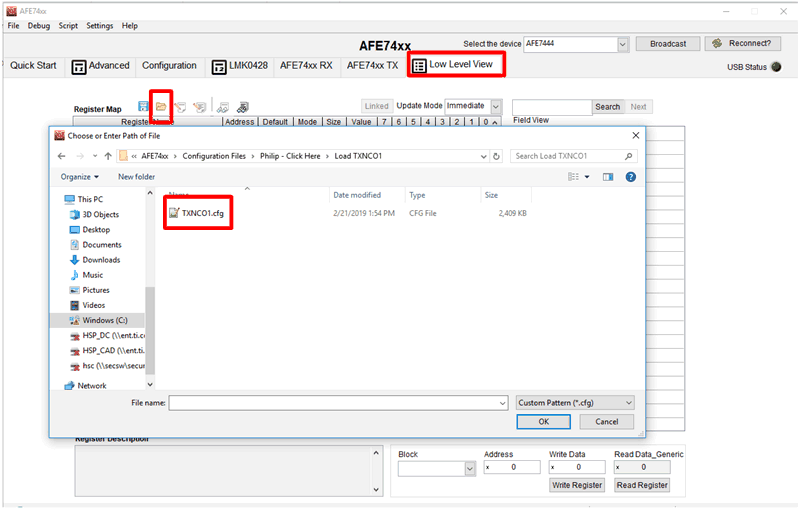
To program TXNCO1 to 1700 MHz, copy the lines of register addresses and values found in Table 1 into a text file, and save the document as a configuration file by adding the .cfg extension at the end of the file name. After the AFE74xx is fully configured in a desired mode, the TXNCO1 configuration file is loaded to the device through the Low-Level tab in the AFE74xx GUI, as shown in Figure 6. The register address for all of the available RX and TX NCOs in the AFE74xx are listed in Section 7.
 Figure 6. Loading the TXNCO1 Configuration File