SLAA870 February 2019 AFE7422 , AFE7444
-
Evaluating the frequency hopping capability of the AFE74xx
- Trademarks
- 1 Introduction
- 2 Phase Coherency vs Phase Continuity
- 3 AFE74xx Architecture
- 4 Frequency Hopping Methods
- 5 NCO Frequency Resolution Versus Hop Time
- 6 Fast Frequency Hopping With the Load and Switch
- 7 Register Addresses
- 8 References
4.2.2.1 Test Setup
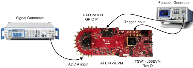
GPIO hop time is calculated using a TSW14J56EVM connected to an AFE74xxEVM. The TSW14J56EVM is a data capture card with an input-trigger feature, where data capture begins as soon as the designated SMA input receives a 1.8-V logic high signal. A function generator connects to both the RXFBNCO0 GPIO pin and the SMA trigger input of the TSW14J56EVM. The function generator outputs a single-pulse square wave at 1 Hz with an amplitude of 1.8 V. The signal from the function generator activates the TSW14J56 trigger and switches the selected NCO from RXNCO0 to RXNCO1. The TSW14J56EVM captures the change in frequency from 100 MHz to 10 MHz as the enabled NCO switches from RXNCO0 to RXNCO1. The test setup for this example is shown in Figure 23.
 Figure 23. Test Setup for Measuring RX NCO Hop Time Using the GPIO Pins