SLAA890A December 2019 – August 2021 MSP430FR2000 , MSP430FR2032 , MSP430FR2033 , MSP430FR2100 , MSP430FR2110 , MSP430FR2111 , MSP430FR2153 , MSP430FR2155 , MSP430FR2310 , MSP430FR2311 , MSP430FR2353 , MSP430FR2355 , MSP430FR2422 , MSP430FR2433 , MSP430FR2475 , MSP430FR2476 , MSP430FR2512 , MSP430FR2522 , MSP430FR2532 , MSP430FR2533 , MSP430FR2632 , MSP430FR2633 , MSP430FR2672 , MSP430FR2673 , MSP430FR2675 , MSP430FR2676 , MSP430FR4131 , MSP430FR4132 , MSP430FR4133
- Trademarks
- 1Overview of the MSP430FR4xx and MSP430FR2xx ADC Module
- 2Comparison Between the FR2xx/FR4xx ADC and ADC12_B
- 3Tailoring the ADC and Reference Voltages to Your Application
- 4Using the Window Comparator to Monitor a Signal Without CPU Intervention
- 5Calibration of VREF and the Internal Temperature Sensor to Improve Performance
- 6FR2xx/FR4xx ADC Example Code and Resources
- 7References
- 8Revision History
3.3 Signal Resolution
Signal resolution determines how accurate a signal can be measured when translated into a digital value since the digital value is finite. The smaller the signal resolution, the better the signal accuracy one can capture. Signal resolution is calculated based on the ADC reference voltage and the number of ADC bits. First, determine your input signal voltage peak-to-peak. Then, select the smallest reference voltage larger than the peak voltage to be captured. This provides the finest signal resolution when calculating it in code. Signal resolution can be calculated using Equation 1.
- n = ADC conversion resolution
Assuming VREF+ = 2.5 V, VREF- = 0 V, and n = 12 bits, the signal resolution can be calculated using Equation 2.
As an example, if your sensor output dynamic range is between 0 V to 1.8 V and you want to use the internal reference, you would select the reference voltage of 2 V. This allows the input signal to not saturate the ADC while providing the finest resolution.
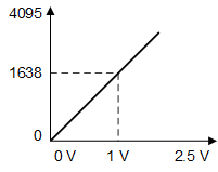
Based on the signal resolution, you can calculate the ideal ADC code from the input voltage. To calculate the ADC code, assuming VREF+ is 2.5 V, 1-V input voltage, and 12-bit resolution, and Equation 3 where Equation 1 has been solved for the signal applies.
 Figure 3-2 Input Signal to ADC Code