SLASE58E February 2016 – December 2019 MSP430FR2310 , MSP430FR2311
PRODUCTION DATA.
- 1Device Overview
- 2Revision History
- 3Device Comparison
- 4Terminal Configuration and Functions
-
5Specifications
- 5.1 Absolute Maximum Ratings
- 5.2 ESD Ratings
- 5.3 Recommended Operating Conditions
- 5.4 Active Mode Supply Current Into VCC Excluding External Current
- 5.5 Active Mode Supply Current Per MHz
- 5.6 Low-Power Mode LPM0 Supply Currents Into VCC Excluding External Current
- 5.7 Low-Power Mode LPM3 and LPM4 Supply Currents (Into VCC) Excluding External Current
- 5.8 Low-Power Mode LPMx.5 Supply Currents (Into VCC) Excluding External Current
- 5.9 Production Distribution of LPM Supply Currents
- 5.10 Typical Characteristics – Current Consumption Per Module
- 5.11 Thermal Resistance Characteristics
- 5.12
Timing and Switching Characteristics
- 5.12.1 Power Supply Sequencing
- 5.12.2 Reset Timing
- 5.12.3 Clock Specifications
- 5.12.4 Digital I/Os
- 5.12.5 VREF+ Built-in Reference
- 5.12.6 Timer_B
- 5.12.7
eUSCI
- Table 5-14 eUSCI (UART Mode) Clock Frequency
- Table 5-15 eUSCI (UART Mode) Switching Characteristics
- Table 5-16 eUSCI (SPI Master Mode) Clock Frequency
- Table 5-17 eUSCI (SPI Master Mode) Switching Characteristics
- Table 5-18 eUSCI (SPI Slave Mode) Switching Characteristics
- Table 5-19 eUSCI (I2C Mode) Switching Characteristics
- 5.12.8 ADC
- 5.12.9 Enhanced Comparator (eCOMP)
- 5.12.10 Smart Analog Combo (SAC)
- 5.12.11 Transimpedance Amplifier (TIA)
- 5.12.12 FRAM
- 5.12.13 Emulation and Debug
-
6Detailed Description
- 6.1 Overview
- 6.2 CPU
- 6.3 Operating Modes
- 6.4 Interrupt Vector Addresses
- 6.5 Memory Organization
- 6.6 Bootloader (BSL)
- 6.7 JTAG Standard Interface
- 6.8 Spy-Bi-Wire Interface (SBW)
- 6.9 FRAM
- 6.10 Memory Protection
- 6.11
Peripherals
- 6.11.1 Power-Management Module (PMM) and On-chip Reference Voltages
- 6.11.2 Clock System (CS) and Clock Distribution
- 6.11.3 General-Purpose Input/Output Port (I/O)
- 6.11.4 Watchdog Timer (WDT)
- 6.11.5 System Module (SYS)
- 6.11.6 Cyclic Redundancy Check (CRC)
- 6.11.7 Enhanced Universal Serial Communication Interface (eUSCI_A0, eUSCI_B0)
- 6.11.8 Timers (Timer0_B3, Timer1_B3)
- 6.11.9 Backup Memory (BAKMEM)
- 6.11.10 Real-Time Clock (RTC) Counter
- 6.11.11 10-Bit Analog-to-Digital Converter (ADC)
- 6.11.12 eCOMP0
- 6.11.13 SAC0
- 6.11.14 TIA0
- 6.11.15 eCOMP0, SAC0, TIA0, and ADC in SOC Interconnection
- 6.11.16 Embedded Emulation Module (EEM)
- 6.11.17 Peripheral File Map
- 6.12 Input/Output Diagrams
- 6.13 Device Descriptors (TLV)
- 6.14 Identification
- 7Applications, Implementation, and Layout
- 8Device and Documentation Support
- 9Mechanical, Packaging, and Orderable Information
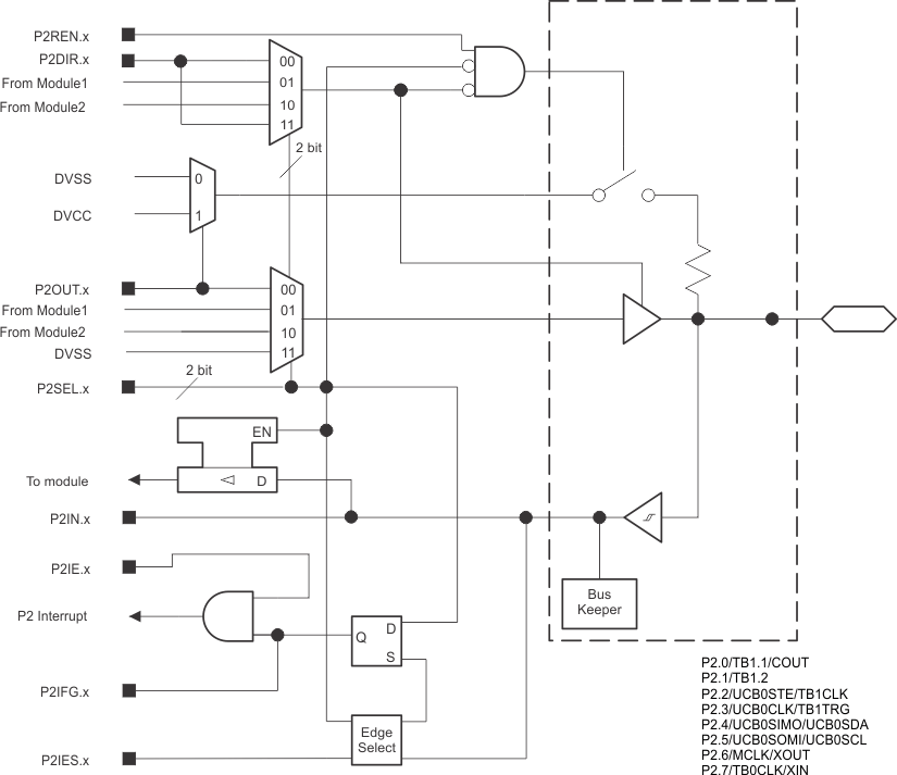
6.12.2 Port P2 Input/Output With Schmitt Trigger
Figure 6-6 shows the port diagram. Table 6-44 summarizes the selection of the port functions.

NOTE:
Functional representation only.Table 6-44 Port P2 Pin Functions
| PIN NAME (P2.x) | x | FUNCTION | CONTROL BITS AND SIGNALS(1) | |
|---|---|---|---|---|
| P2DIR.x | P2SELx | |||
| P2.0/TB1.1/COUT | 0 | P2.0 (I/O) | I: 0; O: 1 | 00 |
| TB1.CCI1A | 0 | 01 | ||
| TB1.1 | 1 | |||
| COUT | 1 | 10 | ||
| P2.1/TB1.2 | 1 | P2.1 (I/O)0 | I: 0; O: 1 | 00 |
| TB1.CCI2A | 0 | 01 | ||
| TB1.2 | 1 | |||
| P2.2/UCB0STE/TB1CLK | 2 | P2.2 (I/O) | I: 0; O: 1 | 00 |
| UCB0STE | X | 01 | ||
| TB1CLK | 0 | 10 | ||
| VSS | 1 | |||
| P2.3/UCB0CLK/TB1TRG | 3 | P2.3 (I/O) | I: 0; O: 1 | 00 |
| UCB0CLK | X | 01 | ||
| TB1TRG | 0 | 10 | ||
| P2.4/UCB0SIMO/UCB0SDA | 4 | P2.4 (I/O) | I: 0; O: 1 | 00 |
| UCB0SIMO/UCB0SDA | X | 01 | ||
| P2.5/UCB0SOMI/UCB0SCL | 5 | P2.5 (I/O) | I: 0; O: 1 | 00 |
| UCB0SOMI/UCB0SCL | X | 01 | ||
| P2.6/MCLK/XOUT | 6 | P2.6 (I/O) | I: 0; O: 1 | 00 |
| MCLK | 1 | 01 | ||
| VSS | 0 | |||
| XOUT | X | 10 | ||
| P2.7/TB0CLK/XIN | 7 | P2.7 (I/O) | I: 0; O: 1 | 00 |
| TB0CLK | 0 | 01 | ||
| VSS | 1 | |||
| XIN | X | 10 | ||