SLAU887 February 2023 MSPM0C1105 , MSPM0C1106 , MSPM0G1105 , MSPM0G1106 , MSPM0G1107 , MSPM0G1505 , MSPM0G1506 , MSPM0G1507 , MSPM0G1518 , MSPM0G1519 , MSPM0G3105 , MSPM0G3105-Q1 , MSPM0G3106 , MSPM0G3106-Q1 , MSPM0G3107 , MSPM0G3107-Q1 , MSPM0G3505 , MSPM0G3505-Q1 , MSPM0G3506 , MSPM0G3506-Q1 , MSPM0G3507 , MSPM0G3507-Q1 , MSPM0G3518 , MSPM0G3518-Q1 , MSPM0G3519 , MSPM0G3519-Q1 , MSPM0H3216 , MSPM0L1105 , MSPM0L1106 , MSPM0L1227 , MSPM0L1227-Q1 , MSPM0L1228 , MSPM0L1228-Q1 , MSPM0L1303 , MSPM0L1304 , MSPM0L1304-Q1 , MSPM0L1305 , MSPM0L1305-Q1 , MSPM0L1306 , MSPM0L1306-Q1 , MSPM0L1343 , MSPM0L1344 , MSPM0L1345 , MSPM0L1346 , MSPM0L2227 , MSPM0L2227-Q1 , MSPM0L2228 , MSPM0L2228-Q1
- Abstract
- Trademarks
- 1Overview of BSL Features
- 2Terminology
- 3BSL Architecture
- 4Bootloader Protocol
- 5Sample Program Flow with Bootloader
- 6Secondary Bootloader
- 7Interface Plug-in
- 8References
- 9Revision History
3.3.1 SRAM Memory Usage
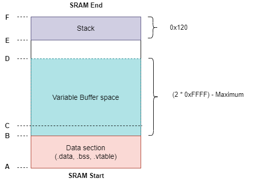
The SRAM Memory layout explains the memory used for bootloader's operation.
- Data and Stack section - Used by BSL for it's operation. While exiting the bootloader, these sections of the SRAM are cleared.
- Variable Buffer Space - Buffer space used for storing the data packets received /sent during the BSL communication
The SRAM memory allowed for read and write access by the host is BSL Buffer Start Address to [SRAM end address - 0x120], where SRAM end address is determined by the SRAM memory available in each device. Since the same SRAM space is shared with variable buffer space, it has chances of getting overwritten during an SRAM write/read operation.
 Figure 3-3 SRAM Usage
A - SRAM Start Address (0x20000000)
B- 'BSL Buffer Start Address' known from the 'Get Device Info' command response, when no Flash plug-in interface is registered
C- 'BSL Buffer Start Address' known from the 'Get Device Info' command response. It will be same as 'B' when no Flash plug-in interface is registered
D- BSL Buffer End Address ='BSL Buffer Start Address' + (2 * 'BSL Max Buffer size'), where BSL Buffer Start Address and BSL Max Buffer Size can be known from 'Get Device Info' command response
E- Start address of the stack allocation (E - 0x120). It will be same as 'D' when the 'BSL Max Buffer size' is less than 0xFFFF
F- End address of the SRAM memory available in the device. Refer to device specific data sheet to know this.
Section B- C :
Data section that will be allocated for Flash Plug-in operation, when registered in BSL configuration
Section C- D:
Buffer space used to store data packets
Maximum size is (2 * 0xFFFF)
Section C-E:
- Available memory for SRAM read and write operation through BSL commands