SLLA565 September   2021 TUSB1044


  1.   Trademarks
  2. 1Introduction
  3. 2TUSB1044 Configuration and Control Implementation
    1. 2.1 TUSB1044 Four-Level Pins
      1. 2.1.1 I2C_EN
      2. 2.1.2 VIO_SEL
      3. 2.1.3 UEQ[1:0] and DEQ[1:0]
      4. 2.1.4 CFG[1:0]
    2. 2.2 TUSB1044 Two-Level Pins
      1. 2.2.1 FLIP, CTL0, and CTL1
      2. 2.2.2 DIR0 and DIR1
      3. 2.2.3 SWAP
      4. 2.2.4 HPDIN
      5. 2.2.5 SLP_S0#
  4. 3TUSB1044 I2C Mode Implementation
    1. 3.1 TUSB1044 Operating Mode Configuration, General_1 Register, 0x0A
    2. 3.2 VOD Configuration, General_3 Register 0x0C
    3. 3.3 Upstream and Downstream Equalization Configuration Registers, UFP1_EQ, UFP2_EQ, DFP1_EQ, and DFP2_EQ Registers 0x10, 0x11, 0x20, 0x21
  5. 4Benefits of Using the I2C Mode Control
  6. 5TUSB1044 Host Implementation Example
  7. 6TPS6598X, TPS6599X Based I2C Control and Tuning
    1. 6.1 Enable PD Controller I2C Control of External Slaves
    2. 6.2 Example of I2C Configuration Upon PD Controller PoR Event and Detach Event
    3. 6.3 Example of I2C Configuration Upon Cable-Orientation Event and DP Configuration Event
    4. 6.4 Notes for Application
  8. 7References

TUSB1044 Host Implementation Example

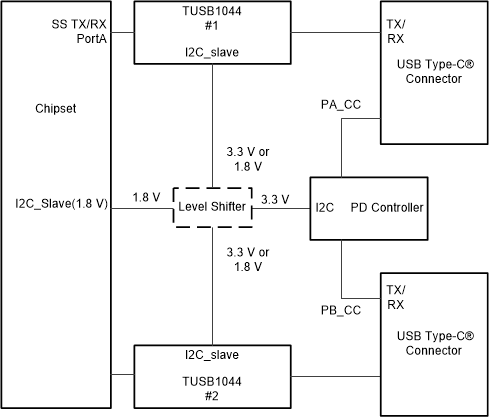
Figure 5-1 shows the TUSB1044 implementation example at the source side. Table 5-1 defines the TUSB1044 pin configuration for this particular example. For AMD platforms, the APU Crossbar and the TUSB1044 are usually controlled by the PD controller using the same I2C bus. Consider using a level shifter to isolate different power rails and to prevent leakage.

Note: The host platform such as AMD where the rated IO voltage is designed to be 1.8 V, “R” needs to be considered for VIO_SEL pin to support the 1.8-V pull-high for I2C.

Since the TUSB1044 upstream is connected to the APU and the downstream is connected to the USB Type-C connector, set the SWAP and DIR[0:1] appropriately as shown in Table 5-1. Note that SWAP and DIR[0:1] can also be controlled through I2C registers.

GUID-20210713-CA0I-3LKG-RKD8-LHLDMRT4QDHW-low.gif

Figure 5-1 TUSB1044 Block Diagram in a DFP System
Table 5-1 TUSB1044 Functional Pins Configurations Example in I2C Mode
Pin # Definition Pin Level
5 Swap 0(Default)
7 SLP_S0# 1(Default)
8 DIR0 0
11 DIR1 0
14 VIO_SEL R
17 I2C_EN 1