SLLU166A June 2012 – September 2022 ISO1540 , ISO1540-Q1 , ISO1541 , ISO1541-Q1
2.2 Input/Output Signal Characteristics
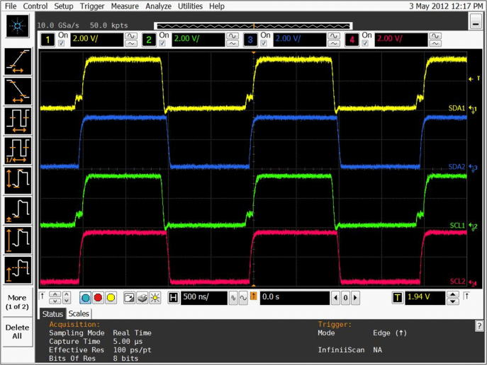
Figure 2-2 illustrates SDA1 and SCL1 of U1 being treated as inputs and driven by an I2C transmitter connected to J3A/J4A (for SDA1) and J5A/J6A (for SCL1). The output waveforms at SDA2 and SCL2 are captured on the oscilloscope at J3B/J4B and J5B/J6B respectively. Note the step in the rising edge of the input waveforms at SDA1 and SCL1 indicative of the tLOOP parameter of the device and demonstrating the effect of the difference in the low levels for the side 1 output and input enabling the device to avoid a latch-up state.

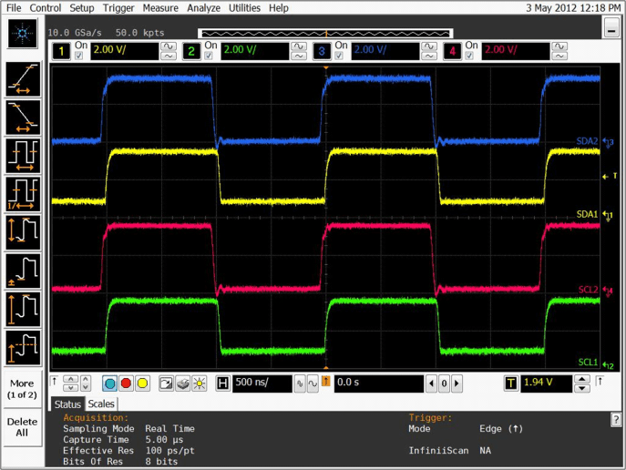
Figure 2-3 illustrates SDA2 and SCL2 of U1 being treated as inputs and driven by an I2C transmitter connected to J3B/J4B (for SDA2) and J5B/J6B (for SCL2). The output waveforms for SDA1 and SCL1 are captured on the oscilloscope at J3A/J4A and J5A/J6A respectively. Note the low level of the SDA1 and SCL1 outputs offset from the ground level. This is due to the high output low level on side 1 designed to prevent a latch-up state.

In addition to the cases shown here, the SDA and SCL signals also propagate in mutually opposing directions. However, if using ISO1541, the SCL line is unidirectional and only allows the signal to propagate from SCL1 to SCL2 and not vice-versa.