SLOA044A March 2000 – June 2021 TL2842 , TL2842B , TL2843 , TL2844 , TL2845 , TL3842 , TL3842B , TL3843 , TL3844 , TL3845 , TLC081 , TLC2201 , TLV2231 , TLV2361 , TLV2362 , TLV2470 , TLV2471 , TLV2770 , TLV2771 , TLV341 , TLV342 , UC1842 , UC1843 , UC1844 , UC1845 , UC2842 , UC2842A , UC2843 , UC2843A , UC2844 , UC2844A , UC2845 , UC2845A , UC3841 , UC3842 , UC3842A , UC3842M , UC3843 , UC3843A , UC3844 , UC3844A , UC3845 , UC3845A , UC3845AM , UCC1800 , UCC1801 , UCC1802 , UCC1803 , UCC1804 , UCC1805 , UCC2800 , UCC2801 , UCC2802 , UCC2802M , UCC2803 , UCC2804 , UCC2805 , UCC2813-0 , UCC2813-1 , UCC2813-2 , UCC2813-3 , UCC2813-4 , UCC2813-5 , UCC28C40 , UCC28C41 , UCC28C42 , UCC28C43 , UCC28C44 , UCC28C45 , UCC3801 , UCC3802 , UCC3803 , UCC3804 , UCC3805 , UCC3813-0 , UCC3813-1 , UCC3813-2 , UCC3813-3 , UCC3813-4 , UCC3813-5 , UCC38C40 , UCC38C41 , UCC38C42 , UCC38C43 , UCC38C44 , UCC38C45
4 Choosing the Op Amp
Size and number of channels:
The op amp chosen is typically a single channel op amp as only one is required. Texas Instruments offers-single channel op amps in SOT-23, MSOP 8-pin, and SOIC 8-pin packages.
Rail-to-rail input or output:
The input signal to the op amp is the sense voltage (Vsense), which is ground referenced. However, the peak voltage of Vsense is typically very low and will not approach the positive power supply voltage of the op amp. Therefore, a rail-to-rail input op amp is not required. All of Texas Instruments single supply CMOS operational amplifiers can accept input signals as low as the ground.
The output signal of the op amp is the Vs signal, which typically swings from 0 V to 1 V. The load current into the PWM IC is typically quite small, and therefore does not significantly limit the choice of op amps. Almost all of Texas Instruments single-supply CMOS op amps are capable of swinging to ground on the output. The load current into the PWM IC is typically quite small, and therefore will not significantly limit the choice of op amps.
Powering the Op Amp:
It is recommended to power the op amp from the reference output of the PWM IC used in the power supply. This reference is often 5.0 V, but can be lower. TI offers single-channel op amps that work from supply voltages as low as 2.5 V, such as the TLV2771. The reference output of the PWM IC (such as the UC384x and UCC380x family of PWM controllers) is often able to supply output drives of several milliamperes, which is adequate to power many op amps. The op amp should be grounded to the same analog ground used by the PWM IC. The current required by the op amp is the ICC current as well as the drive current. A feedback resistor (Rf) value between 10 kΩ and 100 kΩ is recommended to limit the drive current.
Slew rate and gain-bandwidth product:
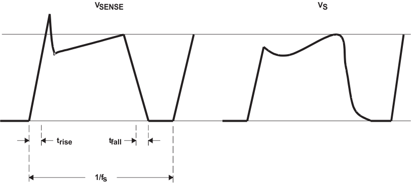
 Figure 4-1 Current Sense Waveforms
Figure 4-1 shows a representation of VSense, the current-sense signal across the sense resistor, and VS, the filtered signal desired at the PWM IC. The leading edge of VSense contains a spike that is due to parasitic elements in the power supply, including reverse recovery of diodes and capacitance of the MOSFET. This spike is undesirable and can be filtered out using the feedback capacitor Cf, as shown in Figure 1-1 (b). The filter time-constant is often set to be three to four times the rise time of this spike. The filter’s pole must be set low enough to filter the leading edge spike, but not so low that the current ramp signal is distorted. The filter pole must therefore be set above the switching frequency (fs) of the switch-mode power supply. This can be expressed as:
So, for a rise time (tr) of 100 ns and a 100-kHz switching frequency, this corner frequency would be set to 400 kHz. In this case the limiting factor is the time constant.
Because the circuit filters out frequencies above fc, the gain-bandwidth (GBW) product of the op amp used can be easily calculated as:
For the earlier example where the gain was set to 15, and with a 400-kHz corner frequency, the GBW for the desired op amp is calculated to be 6 MHz.
The slew rate (SR) of the waveform in Figure 4-1 can be determined by the falling slope, and is equal to VPeak/tfall. However, the bandwidth of the circuit is limited significantly by the RC time-constant of the pole. It can be assumed that the slew rate of the op amp should exceed the limitation of the filter time constant. Therefore, the slew rate can be determined by:
Continuing the earlier example, this would result in a SR of: