SLOA332 july 2023 LMV821-N , LMV831 , OPA2991 , OPA345 , OPA376 , OPA376-Q1 , OPA377 , OPA377-Q1 , OPA4991 , OPA991 , TL074 , TLV376 , TLV9001 , TLV9002 , TS321
- 1
- Abstract
- Trademarks
- 1Slew Rate Definition
- 2Bipolar Op Amp Slew Rate Example
- 3CMOS Op Amp Slew Rate Example
- 4Four Methods to Determine Boost or No Boost Using the Data Sheet
- 5Slew Rate Dependencies on Circuit Signal Levels and Op Amp Gain Set by Feedback Network
- 6How Much Output Slew Rate is Needed to Support a Sine Wave or Other Non-step Inputs
- 7Stability Also Plays a Role in Observed Slew Rate
- 8Summary
- 9References
4 Four Methods to Determine Boost or No Boost Using the Data Sheet
Method 1: Compare Slew Rate Versus Gain Bandwidth
The first method is to compare the slew rate (SR) in V/µs to the gain bandwidth product (GBWP) in MHz. If the SR > GBWP, then slew boost is likely integrated in the device. If SR < GBWP, then boost is not as likely to be integrated into the device. TLV9001 has SR > GBWP, (2 V/µs > 1 MHz), which indicates that boost is likely integrated into the device. LMV831 has SR < GBWP, (2 V/µs < 3.3 MHz), which indicates that boost is not likely to be integrated in the device.
| Boost | No Boost |
|---|---|
| Device TLV9001 | Device LMV831 |
| Slew rate 2 V/µs | Slew rate 2 V/µs |
| Bandwidth 1 MHz | Bandwidth 3.3 MHz |
Method 2: Compare Quiescent Current Versus Similar SR Devices
The second method is to compare the quiescent current (IQ) per channel to other op amps that have similar supply voltage maximums and similar slew rates. IQ and GBWP are proportionally related. If IQ is very low or part of a lower bimodal distribution, then slew boost is expected. If IQ is near the median or above the median value, then boost is not expected. TLV9001 has a very low IQ, which makes boost very likely. LMV831 is lower than the median IQ value, but much greater then the lowest IQ, therefore, boost or no boost is inconclusive using this test.
| Part Number | Iq/CH (mA) | GBWP (MHz) | SR (V/µs) | Boost? |
|---|---|---|---|---|
| TLV9001 | 0.06 | 1 | 2 | Likely |
| LMV831 | 0.25 | 3.3 | 2 | Inconclusive |
| LMV821-N | 0.30 | 5.6 | 2 | Inconclusive |
| OPA377 | 0.76 | 5.5 | 2 | No |
| OPA376 | 0.76 | 5.5 | 2 | No |
| TLV376 | 0.82 | 5.5 | 2 | No |
Method 3: Evaluate Large Signal Response
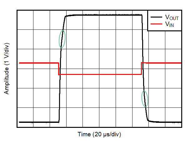
Use any large signal chart that has abrupt changes in rise and fall slopes, including charts called by another name, such as “Overload Recovery”. If a chart with these conditions can not be found, use the chart with the largest input signal. When looking at the transient response, select the slowest slew rate section that is more than 100 mV of VID. Taking into account the noise gain (NG) of the circuit, the slowest slew rate section for a NG of 11 is 1.1 V and for a NG of 1 the VID is 100 mV. As shown in Figure 4-1, the green ovals are the slowest slew rate with full VID. In both waveforms there is initially a faster slew rate. This initial increased slew rate can be caused by slew boost or internal parasitic capacitive feed-through. Typically, small rises come from capacitive feed-through and large rise come from slew boost. For the TLV9001 waveform, the selected area (SR) is 0.6 V/µs, which is less than half of the data sheet slew rate of 2 V/µs. Based on this information, slew boost is present in the TLV9001. For the LMV831 waveform, the selected area (SR) is 2.2 V/µs rising and 1.8 V/µs falling SR, which is close to the data sheet slew rate of 2 V/µs; therefore, so no boost is expected.
| Boost | No Boost | |
|---|---|---|
| Device | TLV9001 | LMV831 |
| NG | 11 | 1 |
| VIN | 600 mV | 500 mV |
| Selected SR | 0.6 V/μs | +2.2, -1.8 V/μs |
| Data sheet SR | 2 V/μs | 2 V/μs |
 Figure 4-1 TLV9001 Overload
Recovery
 Figure 4-2 LMV831 Large Signal Step
Response With Gain = 1
Figure 4-2 LMV831 Large Signal Step
Response With Gain = 1Method 4: Evaluate Small Signal Response
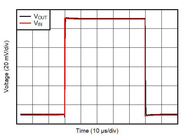
The fourth method is to evaluate the SR in small input signal charts. Use the chart with the smallest input signal and highest noise gain. It can be necessary to zoom in to accurately measure the waveform relative to division scaling to get the initial slew rate after any internal capacitive-forward coupling. The time division of the TLV9001 waveform is too long, making the rise and fall appear to be vertical lines, so it is not possible to determine waveform SR with any accuracy. The TLV9001 waveform does not indicate boost or no boost. The LMV831 waveform is a great waveform to use as an indicator because the input is small, NG is high, and scaling makes rise and fall time measurable. The initial slew rate is consistent with the rest of the rising slew rate, so this section can be used for evaluation. Initial SR of the green oval area is 0.25 V/µs. The 10-mV VID translates to 14% SR[max] using Figure 3-1. The data sheet value (2 V/µs) scaled by 14% is 0.28 V/µs. The small signal slew rate of the waveform, 0.25 V/µs, closely matches the calculated slew rate, 0.28 V/µs. Based on these calculations, the LMV831 device does not have slew boost.
| Result | Inconclusive | No Boost |
|---|---|---|
| Device | TLV9001 | LMV831 |
| NG | 1 | 10 |
| VIN | 100 mV | 10 mV |
| Initial SR | Unknown | 0.25 V/μs |
Data sheet SR × Figure 3-1 output | 1.8 V/μs | 0.28 V/μs |
 Figure 4-3 TLV9001 Small Signal Waveform
 Figure 4-4 LMV831 Small Signal Waveform