SLUA749A July 2015 – May 2016 BQ76920 , BQ76930 , BQ76940
10 Random Cell Connection – Within Limits
The bq769x0 datasheet feature list includes “Random cell connection tolerant”. The user may be left wondering what this means since there are no specifications related to the cell connection. Basically the part was designed to not have pins excessively sensitive to transients during cell connection if the currents into the pins are limited by appropriate resistances. This does not mean that the abs maximum limits can be completely ignored or that the part can take unlimited abuse. Differences in implementations may vary the stress on the IC during cell connection and tolerances may also result in differences between successful assembly and damage. The bq76920 is typically more durable in connection than the bq76930 or bq76940 since all cell inputs are in one group and bounded by the power pins.
Connection of the cells assumes connection of the device VSS first since signals in the IC are referenced to VSS. VSS will typically be connected to the high current path of the board and would be connected to battery-. In some cases VSS is connected to battery- through a low current ground.
Generally a bottom-up cell connection sequence is preferred since the voltage step applied to the board with each connection is small. The voltage on the input will charge the filter capacitor for that cell. The differential filter capacitors will push up the unconnected upper cells. Additionally the body diodes of the IC’s internal balance FETs will push up the unused input if they conduct. If external balance FETs are used their body diode will also push up the upper cell terminals through the cell balance resistors. Another cell connection method which is sometimes preferred is to connect the VSS followed by the cell which provides the group power, cell 5 for example in a 5 cell battery. This provides a large voltage step size to the board but defines the power for the group, the differential input filter capacitors divide the voltages to the intermediate pins. Connecting a cell in the middle of the group after the connection of the power will provide a slight correction of the IC pin voltage from the value resulting from the capacitor divider. Unconnected cell inputs are free to drift based on IC pin and capacitor leakages. As with any assembly technique, care should be taken to be sure unconnected inputs do not contact damaging voltages before their connection. This connection of the group power second (after VSS) may be preferred when there is a heavy load on the power such as may be the case with a bq76920 where there is a regulator running on battery+ which might push a high current through the balance FETs during a bottom up sequence. When a cell in the middle of the group is connected after the VSS, a combination of the two effects described above will occur: inputs for unconnected cells above will be pushed up, inputs for unconnected cells below will be divided by the differential capacitor divider.
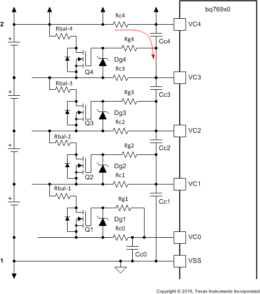
The external balance circuit used can have an effect on the inputs during cell connection. When P-channel FETs are used for balancing, the inrush current through the input filter resistor will turn on the balance FET. If the cell input below is unconnected, the balance FET will pull up the lower unconnected input. This sequence will continue down the input filter as shown in Figure 18. If the VC0 input is not connected to battery-, it can be pulled to a high voltage. While no damage was observed at TI from this condition in limited testing, connecting the bottom of cell 1 input to VSS on the board at least during cell connection is recommended. N-channel balance FETs do not turn on with a higher-input-after-VSS connection since current into the input resistor raises the upper balance FET source voltage above its gate voltage, see Figure 19. These may be preferred for random cell connection since they do not pull unconnected inputs up. If the N-channel FETs were triggered during connection they would pull an input down, this is generally considered safer than a pull up since single ended abs max limits are referenced to VSS, as long as differential limits are not exceeded.
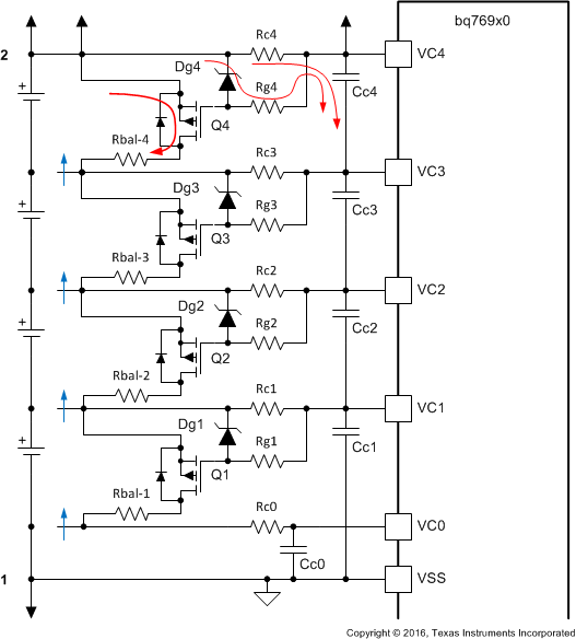 Figure 18. Connection With P-Channel Balance FETs
 The typical application schematics in the datasheet for the bq76930 and bq76940 show diodes from the top input of each group to the group power pin. These diodes are important to prevent damage during random cell connection. Without the diode connection of a cell in an upper group will quickly bring that input to a high level while dividing the input voltages to the group power reference pin. The group power reference pin would not move much due to the large Cf required for the architecture and the connected pin may easily exceed its abs max value to the group reference, see Figure 20. Typical damage to the part from this condition leaves the top cell unable to measure high voltage. The diodes hold down the input force current to charge the power filter path as the input rises. Standard signal or switching diodes are suitable for this application. The peak current in the diodes will be limited by the input resistors. With a 1-kΩ Rc resistor with the maximum recommended 5V/cell on VC15, the current would be 75 mA. Current into Cell 10 with a similar condition would be 50 mA
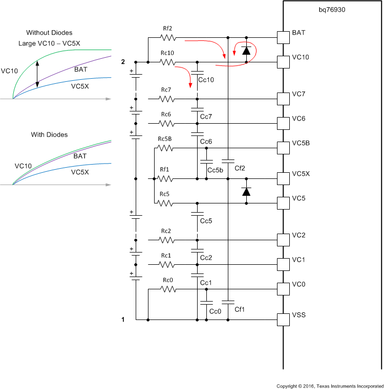 Figure 20. Top Input to Group Power Diodes
 The lower cell input pins on the cell groups have the lowest single ended abs max limits at 3.6 and 7.2 V. The internal balance FET on the bottom cell is necessarily different from the top cell since it must operate at the group reference (ground) while the upper cells operate well above the reference. The bottom internal balance FET meets the same specifications as the other internal FETs but is different and may tolerate transients differently. When a connection is made to a bottom cell input of an upper group, the input will rise quickly from the Rc and Cc filter values, the power reference will rise more slowly through the charge path of the upper cell input filter capacitors and power filter capacitors. The bottom of the group sense pin (VC5B, VC10B) could be 6 diode drops above the group power pin, the lower cell sense pin (VC6, VC11) could be 5 diode drops above the group power pin. The reference for the group would be divided from the group power pin by the power filter capacitors. While TI has not experience damage from cell connection in limited testing, the potential voltage could be large and results may vary with different filter capacitors. Some pack designers have found value in zener diodes on the bottom inputs of the group to the group reference or a zener across the inputs. An example is D11 and D10B shown in Figure 21
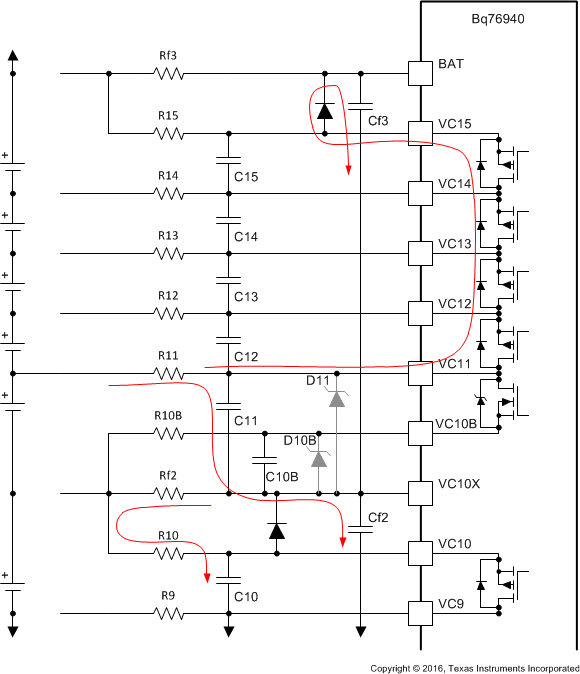 Figure 21. Limiting Lower Group Pin Voltages
 One possibility to help protect the pack inputs is to provide a zener across each cell input. Such zeners can help but may not prevent all issues. Zeners placed at the board inputs must have a nominal breakdown above the cell maximum value and will have a tolerance. These zeners can keep the board differential inputs from an excessive value, but If there is a 0.5V allowance between the maximum cell voltage and the zener conduction point, and if the cells are connected at 0.5V below maximum voltage, each input could accumulate a 1V error. Also realize that with the filter the IC input pins can have a different voltage than the board inputs. Placing zeners at the IC inputs is also possible and can help control voltage swings, however the voltages at the IC inputs will be approximately 1.5 to 2 times the cell voltage during cell balancing depending on the algorithm used.
When possible, connecting zeners to the board in an assembly fixture during assembly may allow a tighter tolerance during connection which would be unacceptable if left in the product during operation while avoiding the cost of the parts in the product. Resistors can also be used to divide the voltage during connection. Resistors would be unacceptable in a product and must be used carefully in a fixture. If the connection to the top cell of a resistor divider is broken, the divider may hold the next to top cell at 0V while the top input goes to the full pack voltage.
Related to the random cell connection, the placement of the IC "ground" may affect the signals on the pins. Parasitics in the high current connection to battery- can cause transients against which the IC may need protection. A resistance between the sense resistor and battery- can cause a voltage drop. If the value is too large, the IC could be damaged. If VSS is referenced near the sense resistor, VC0 will tend to go below ground if connected to the cell and may need protection such as DVC0 in Figure 22. If VC0 is connected on the board, it will not vary significantly from VSS, but the parasitic effect will be included in the bottom cell measurement and VC1 may need protection, see Figure 23. If VSS is referenced to a low current cell 0 connection, the SRP and SRN sense inputs may rise above VSS and transient protection may be required as shown in Figure 24. Note that the recommended operating range of the SRP pin is small, a large path resistance in the will increase the common mode voltage at the SRP and SRN pins.
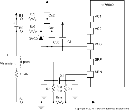 Figure 22. Ground at Sense Resistor and Remote Cell Sense
 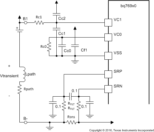 Figure 23. Ground at Sense Resistor and Local Cell Sense
 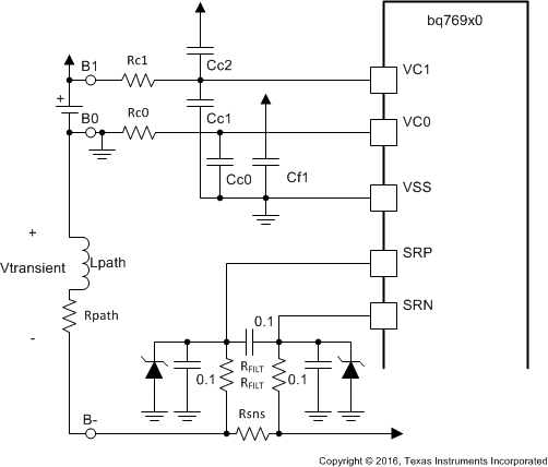 Figure 24. Ground at Remote Cell Sense