SLUA749A July 2015 – May 2016 BQ76920 , BQ76930 , BQ76940
9 REGSRC Supply
REGSRC is a power supply pin separate from the BAT pin which is used to provide power for the FET outputs, and internal circuits such as the coulomb counter and I2C interface as well as any external load through the REGOUT regulator. The FET outputs and REGOUT are provided by internal linear regulators, so the available voltage for the FET drive will be limited by the applied REGSRC voltage. Low voltage packs should use appropriate low gate voltage protection FETs. Power dissipation in the part will also depend on the REGSRC voltage, the REGOUT voltage option and the applied REGOUT load. Figure 12 shows the available FET voltage and nominal dissipation in the IC with a 3.3V REGOUT option and a continuous 20mA load over the recommended input voltage range for REGSRC is 6 to 25V. Dissipation for the 2.5V device output would be higher. Average dissipation with a duty cycled load would be lower. For best FET performance, a higher voltage is desired, for low internal dissipation a low voltage is desired. The best compromise for the device may be to provide a constant supply at approximately 13 to 15V, but this will not typically be available in the battery. Where the power dissipation excessively heats the part or high efficiency is required in the battery, it may be desirable to provide the low voltage load through a separate regulator. REGOUT is used internal circuitry also so it must have a capacitor even if it is not used for external loads.
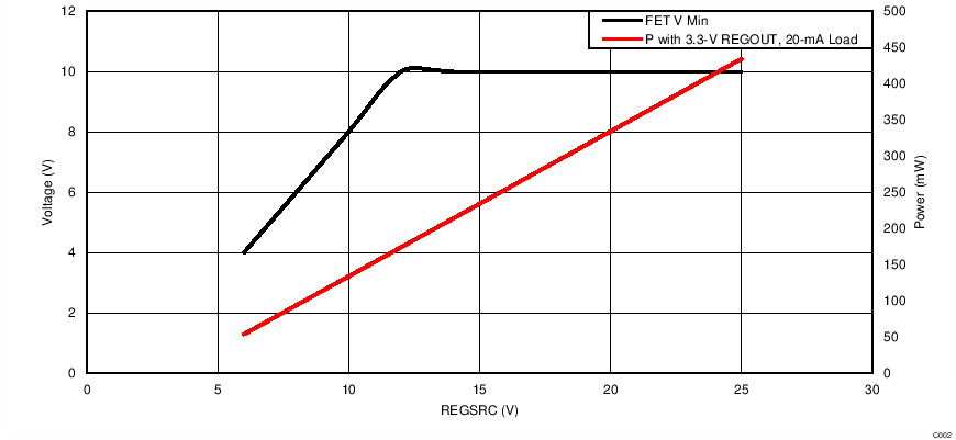 Figure 12. Minimum FET Voltage and Device Dissipation vs. REGSRC
 With the bq76920, the REGSRC pin has the same recommended range as the BAT pin. These pins can generally be tied together to share the same power filter as shown in Figure 13. When a heavy load or short circuit is applied the diode prevents rapid discharge of the BAT and REGSRC pins so that the IC can continue to operate to time the load or short circuit event and with sufficient REGSRC voltage to maintain the FET drive outputs for a good VGS and low resistance from the FETs. While there is not a value in the recommended operating conditions table, it is expected that the BAT pin voltage is normally approximately the same value as the top cell. When the load on the REGOUT pulls the REGSRC pin down significantly, a separate filter can be used on the REGSRC pin to avoid pulling down BAT. As discussed with the BAT pin voltage a zener may be required from the REGSRC pin to VSS to avoid over voltage in some cases.
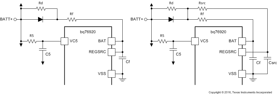 Figure 13. bq76920 REGSRC Power Option
 With the bq76930 and bq76940, the BAT pin voltage may be significantly higher than the maximum acceptable voltage for REGSRC. The datasheet shows using a FET referenced to the VC5X voltage as a source follower. This topology allows REGSRC to operate approximately VGSTH of the FET below the VC5X voltage. FETs are voltage controlled, so the cell stack is not imbalanced by the connection. Current for REGSRC comes from the top of the cell stack, voltage is dropped across the source follower FET. A diode is desired in the path to prevent REGSRC from dropping during heavy load or short circuit as shown in Figure 14. A resistor across the diode will help discharge any transient detected by the diode. The source follower and any dropping components will create an offset between the gate reference and REGSRC voltage. The reference voltage will vary over the dynamic range of the battery, and while that may keep REGSRC in the recommended operating range, it may have an effect on the available FET drive voltages, see Figure 15 If the diode-resistor pair is placed in the source path the voltage drop on the diode with load will reduce the voltage at REGSRC and power dissipated inside the IC, but the REGSRC voltage drop at low cell voltage may have an undesired effect on the FET drive voltages. Placing the diode-resistor pair in the drain path will allow a higher voltage on REGSRC at lower cell voltages. The drain resistor will isolate the FET from ESD on the PACK+ and will reduce power in the FET, but should not be so large that it causes FET source and REGSRC to drop.
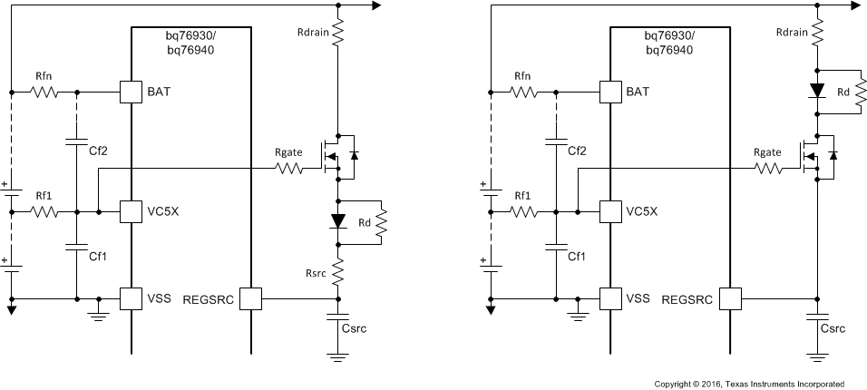 Figure 14. REGSRC Source Follower
 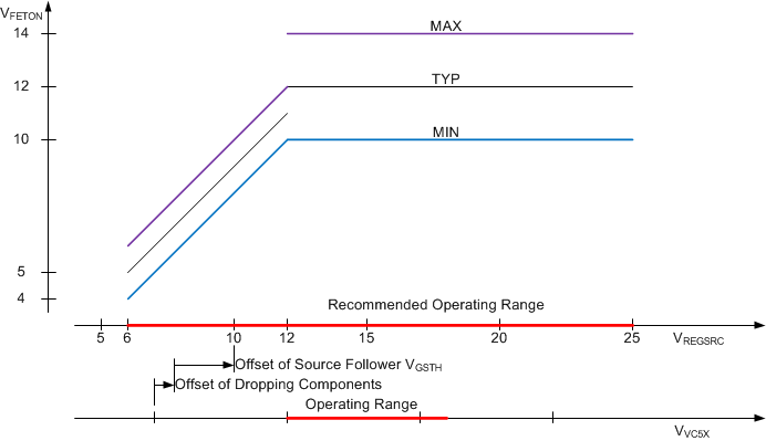 Figure 15. FET Voltage Variation With REGSRC Offset
 For low cell voltages and low cell counts, it may be possible to filter the PACK voltage directly for REGSRC as shown in Figure 16. For the bq76940 there may be cases where using the VC10X as a reference for the source follower gate reference may be suitable. A zener reference would provide a stable voltage reference for the source follower, but would generally be undesired in a battery due to the continuous bias current for the zener. VC5X and VC10X are already heavily filtered and attractive references, but in some cases filtering another cell to provide the gate reference might better fit the needs of REGSRC over the dynamic range of the battery. When the reference voltage for a source follower is at a voltage potential greater than the VGS limit of the FET, protecting the gate with back to back zener diodes may be desired such as shown in Figure 17.
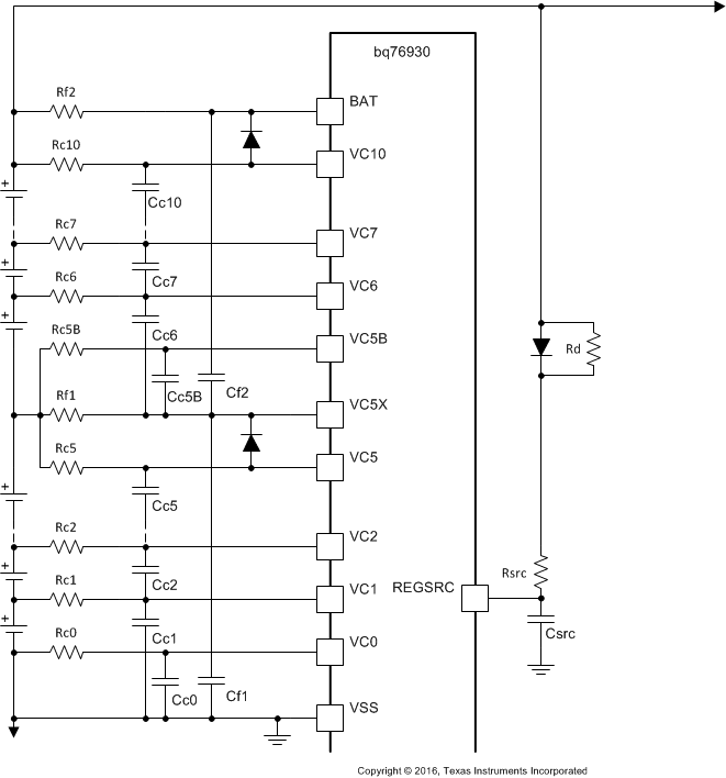 Figure 16. REGSRC From BAT With 6 Cells
 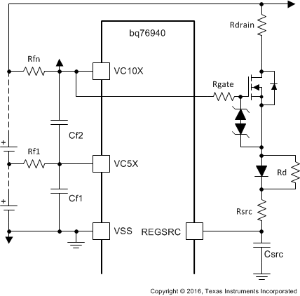 Figure 17. bq76930/bq76940 REGSRC