SLUA778A June 2016 – July 2016 UCC21520 , UCC21520-Q1 , UCC21540
1 Introduction
To fully enhance the performance of the latest high-voltage power semiconductors, such as super junction MOSFETs, trench/field stop IGBTs, wide band-gap SiC and GaN transistors, a universal gate driver becomes a critical interface which not only supports enough peak source/sink current, but also facilitates fast dynamic response with robustness and protection for higher switching frequency and higher efficiency applications.
The flexible, universal capability of the UCC21520 with up to 18-V VCCI and 25-V VDDA/VDDB allows the device to be used as a low-side, high-side, high-side/low-side or half-bridge driver with MOSFETs, IGBTs or SiC MOSFETs. With its integrated components, advanced protection features (UVLO, deadtime and disable) and the optimized dynamic performances, the UCC21520 enables designers to build smaller, more robust designs for enterprise, telecom, automotive and industrial applications allowing for faster time to market.
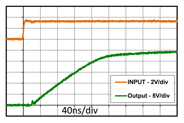
The two output buffer stages of UCC21520 provides 4-A source and 6-A sink current, which provides satisfied rising and falling time (<30 ns) with load capacitance up to 10 nF. However, in some scenarios where the load is larger than 10 nF, external totem-pole buffer stage with discrete transistor should be applied for achieving required rising and falling switching time. Figure 1 shows the UCC21520 drives 30 nF with single channel (green), and the rising time is 110 ns from 5 V to 20 V on the output waveform, which is too long and does increase the switching loss. UCC21520 has two identical designed channels with both propagation delay matching and pulse width distortion less than 5 ns, which make it possible to parallel the output channel and double the gate drive strength. This application note will investigate the dynamic performance of the UCC21520, and also discusses feasibility of paralleling UCC21520 two output channels.
 Figure 1. Single Channel Driving 30-nF Load Capacitance