SLUA778A June 2016 – July 2016 UCC21520 , UCC21520-Q1 , UCC21540
4.1 UCC21520 Efficiently Drives Heavy Capacitive Loads by Paralleling its Output Channels
To further evaluate the UCC21520 with two output channels in parallel, two test setups are prepared to investigate the performance difference. As discussed in Section 2, extra power loss introduced by propagation delay mismatch will add to the typical power consumption.
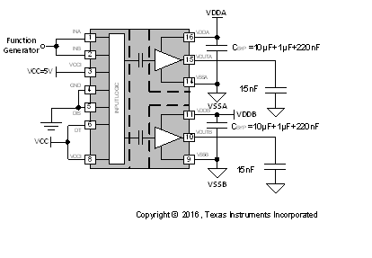 Figure 9. Setup A: UCC21520 Drives Two 15-nF Loads with Two Channels Separately
 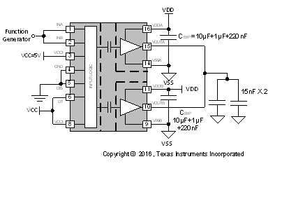 Figure 10. Setup B: UCC21520 Two Channel in Parallel Drives Two 15-nF Load
 Figure 11 through Figure 13 show the total VDD (VDD = 12 V and 25 V) operating current consumption measurement with different switching frequencies at 25°C/-40°C/125°C ambient temperatures. And it can be seen that the current consumption differences between these two setups is negligible.
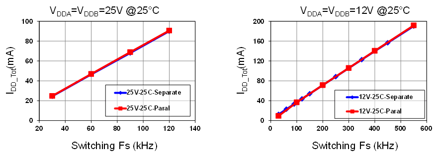 Figure 11. VDD Total Operating Current vs. FS at 25°C
 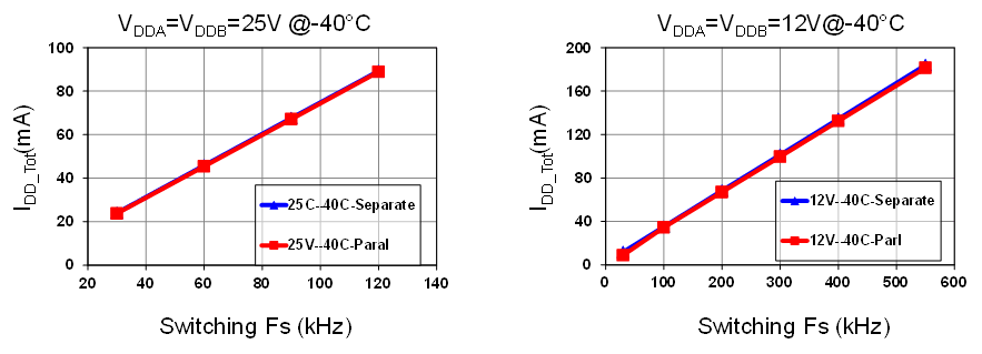 Figure 12. VDD Total Operating Current vs. FS at –40°C
 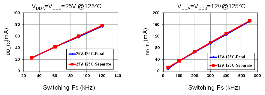 Figure 13. VDD Total Operating Current vs. FS at 125°C
 Figure 14 puts the current consumption data with tri-temperature performance in one graph with zoom-in on the vertical axis.
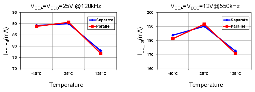 Figure 14. VDD Total Operating Current vs. Temperature at VDD = 12 V and 25 V
 Importantly, the VDD total current consumption data is measured with the device under test (DUT) operating (switching) within only a short moment after the DUT, as well as junction temperature, soaks to the ambient temperature, and the UCC21520 is not running into thermal stable state at the given switching and load condition. The major purpose is to validate the driver device performance at given junction temperature, and the users should not try to run the test conditions for a long time, since it may damage the UCC21520 due to overheating. For UCC21520 safety-related performance, please refer to UCC21520 datasheet.
In summary, the UCC21520 shows very good performance with two output channels in parallel at all operating switching frequencies, VDD range and temperature corners. Due to the best-in-class propagation delay matching performance, the internal shoot-through caused extra loss is negligible. Figure 15 shows the UCC21520 driving 30 nF with parallel and separate output, and it can be seen that the output parallel can effectively increase the gate drive strength by 50%. The rising time is decreased to be 50 ns from 5 V to 20 V on the output, which is less than half when using only single channel.
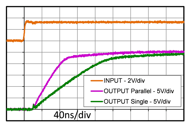 Figure 15. UCC21520 Single Channel Driving 30-nF Load Capacitance