SLUAA81A October 2020 – February 2022 BQ769142 , BQ76922 , BQ76942 , BQ76952
5 Timing Information
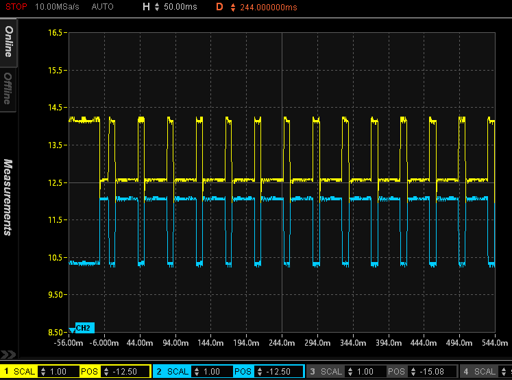
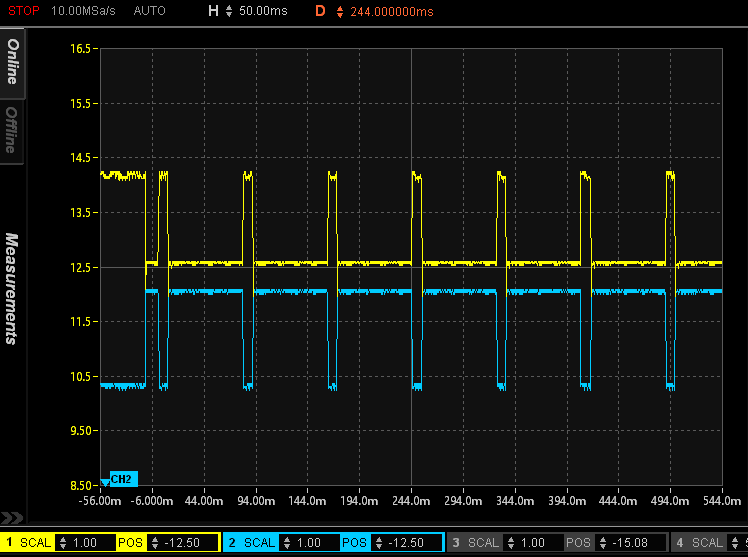
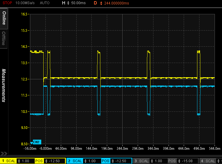
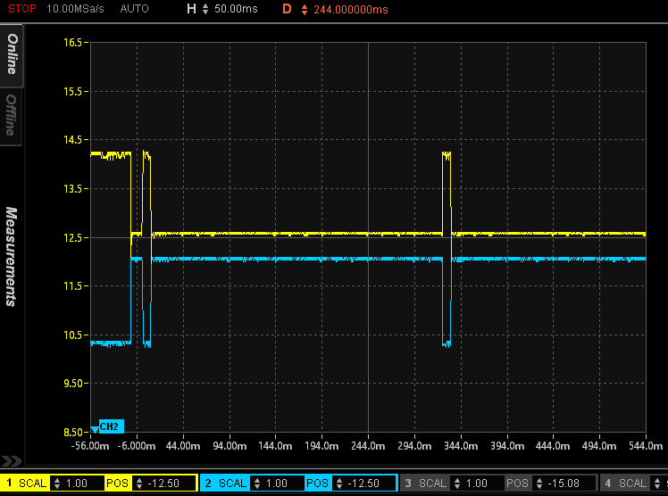
Due to the current that flows into the cell input pins on the BQ769x2 device while balancing is active, the measurement of cell voltages and evaluation of cell voltage protections by the device is modified during balancing. Balancing is temporarily disabled during the regular measurement loop while the actively balanced cell is being measured by the ADC, as well as when the cells immediately adjacent to the active cell are being measured. Similarly, balancing on the top cell is disabled while the stack voltage measurement is underway. This occurs on every measurement loop, and so can result in significant reduction in the average balancing current that flows. In order to help alleviate this, the Settings:Configuration:Power Config[CB_LOOP_SLOW_1:0] configuration bits cause the device to slow the measurement loop speed when cell balancing is active, as shown below. The BQ769x2 devices will insert current-only measurements after each voltage and a temperature scan loop to slow down voltage measurements and thereby increase the average balancing current.
| CB_LOOP_SLOW_1 | CB_LOOP_SLOW_0 | Description |
|---|---|---|
| 0 | 0 | Measurement loop runs at full speed during balancing. |
| 0 | 1 | Measurement loop runs at half speed during balancing. |
| 1 | 0 | Measurement loop runs at quarter speed during balancing. |
| 1 | 1 | Measurement loop runs at eighth speed during balancing. |
In order to avoid the balancing current causing a protection alert or fault, the device modifies the timing on the CUV check on an actively balanced cell and the COV checks on adjacent cells, disabling balancing briefly every 1-sec to allow these checks to occur. If a CUV or COV alert is detected at the 1-sec check, balancing is immediately disabled. Note: the device will therefore have a different delay (≈1-sec) in triggering a CUV or COV alert or fault on these cells while balancing is active. Timing for CUV and COV on other cells besides these being actively balanced or adjacent are not modified.
The device includes an internal die temperature check, to disable balancing if the die temperature exceeds a programmable threshold. However, the customer should still carefully analyze the thermal effect of the balancing on the device in system. Based on the planned ambient temperature of the device during operation and the thermal properties of the package, the maximum power should be calculated that can be dissipated within the device and still ensure operation remains within the recommended operating temperature range. The cell balancing configuration can then be determined such that the device power remains below this level by limiting the maximum number of cells that can be balanced simultaneously, or by reducing the balancing current of each cell by appropriate selection of the external resistance in series with each cell.
While autonomous cell balancing is underway, the conditions related to continuing or stopping balancing are re-evaluated at each Cell Balance Interval. During SLEEP mode, this re-evaluation is done using the data available at the time, which is only updated every Power:Sleep:Voltage Time. Thus, there may be some delay related to these settings before balancing is changed based on the data.
 Figure 5-1 Cell Balancing With CB_SLOW = 0x00,
Cell 4 (yellow) = 3.7 V, Cell 3 (blue) = 3.5 V
 Figure 5-2 Cell Balancing With CB_SLOW = 0x01,
Cell 4 (yellow) = 3.7 V, Cell 3 (blue) = 3.5 V
 Figure 5-3 Cell Balancing With CB_SLOW = 0x10,
Cell 4 (yellow) = 3.7 V, Cell 3 (blue) = 3.5 V
 Figure 5-4 Cell Balancing With CB_SLOW = 0x11,
Cell 4 (yellow) = 3.7 V, Cell 3 (blue) = 3.5 V