SLUAA81A October 2020 – February 2022 BQ769142 , BQ76922 , BQ76942 , BQ76952
2.1 Internal Cell-Balancing Circuit Design
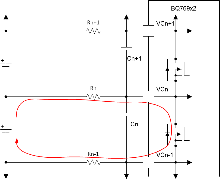
When one of the internal balance FETs is enabled, the internal FET will pull the pins for that cell together drawing current through the input resistors for that cell. The recommended minimum value of the input filter resistors when using internal balancing is 20 Ω. This value maximizes the balance current while keeping it well within the absolute maximum cell balancing current over the internal FET RDS(ON) range. The maximum recommended value for the input filter resistors is 100 Ω.
The typical internal cell balancing resistance (RDS(ON) for the internal FET) is 25 Ω. For a typical lithium ion cell with a full charge voltage of 4.2 V, this results in a balancing current of approximately 65 mA. This is the DC current if the switch was on continuously, so the average balancing current will be lower. The duty cycle is determined by a multiple factors is discussed in more detail in Section 5.
I_Balance = VCell / (2 x Rn + RCB) = 4.2 V / (2 x 20 + 25) ~= 65 mA
 Figure 2-1 Application Circuit for
Internal Balancing
Figure 2-1 Application Circuit for
Internal BalancingFor many applications, the internal balancing current for the device is sufficient and additional external components are not required. However, one must consider the power dissipation and the resulting impact on the device temperature. For example 65 mA into 25 Ω results in about 0.1 W. The junction to ambient thermal resistance for the device is 66 °C/W. If 5 cells are balancing at the same time, this can result in a junction temperature rise of 33 °C.
There are multiple ways to avoid excessive power dissipation. The maximum number of cells allowed to balance simultaneously can be limited by setting Settings: Cell Balancing Config: Cell Balance Max Cells. There are also parameters to control when balancing is allowed based on the cell temperature or the internal temperature of the device. These parameters are available to control power dissipation and temperature in autonomous mode. The cell input resistors values can also be increased to reduce balancing current which will also reduce power dissipation.