SLUAAJ7 June   2022 UCC256402 , UCC256403 , UCC256404


  1.   Abstract
  2.   Trademarks
  3. 1UCC25640x Selection Guide
  4. 2UCC25640x Features Brief Overview
    1. 2.1 High Voltage(HV) Startup
      1. 2.1.1 HV Startup Procedure
      2. 2.1.2 HV Startup with External Bias
      3. 2.1.3 HV Start-up, VCC, X-cap Discharge Internal Block Diagram
      4. 2.1.4 HV Startup External Resistor
    2. 2.2 XCAP Discharge
      1. 2.2.1 IEC Standards
      2. 2.2.2 Detecting AC presence
      3. 2.2.3 Test Current Injection for Zero Crossing Detection
      4. 2.2.4 Typical Waveforms of HV Startup and XCAP Discharge
    3. 2.3 Feedback Chain
      1. 2.3.1 FBreplica Generation
      2. 2.3.2 Vcomp Signal and Threshold Voltages
      3. 2.3.3 FB Pin Voltage Typical Waveform at no Load
    4. 2.4 Hybrid Hysteretic Control and VCR Pin Voltage and Gate Pulse Generation
      1. 2.4.1 Hybrid Hysteretic Control
      2. 2.4.2 VCR Pin Voltage
      3. 2.4.3 VCR Typical Waveform
    5. 2.5 Soft Start
      1. 2.5.1 Soft Start Timing
      2. 2.5.2 Soft Start Initial Voltage Programming
    6. 2.6 Burst Mode
      1. 2.6.1 Burst Patterns
      2. 2.6.2 BMTL/BMTH Ratio Programming
      3. 2.6.3 BMTH Generation
      4. 2.6.4 Interpreting BMTL and BMTH
      5. 2.6.5 Soft On or Off
      6. 2.6.6 Operation when Burst Mode Disabled
      7. 2.6.7 Typical Waveforms
    7. 2.7 Adaptive Dead Time Control
    8. 2.8 Fault Management
      1. 2.8.1 OCP Protection
      2. 2.8.2 OCP Fault Typical Waveforms
      3. 2.8.3 Over Voltage Protection using Bias Winding (BW OVP)
      4. 2.8.4 Restart or Latch
    9. 2.9 ZCS Region Prevention Scheme
      1. 2.9.1 ZCS Effects
      2. 2.9.2 ZCS Detection and Prevention and Disabling
  5. 3UCC25640x Power Up Guidelines and Debugging Notes
    1. 3.1  Power Up Procedure
    2. 3.2  HV Pin
    3. 3.3  VCC Pin
    4. 3.4  BLK Pin
    5. 3.5  FB Pin
    6. 3.6  ISNS Pin
    7. 3.7  VCR Pin
    8. 3.8  BW Pin
    9. 3.9  LL/SS Pin
    10. 3.10 LO Pin
    11. 3.11 RVCC Pin
    12. 3.12 HS, HO, HB Pins
  6. 4References

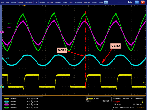
VCR Typical Waveform

GUID-20220530-SS0I-PC0N-C656-VGKXCGTNVCKN-low.png Figure 2-18 Ch1 – LO, Ch2 – VCR, Ch3 – ISNS, Ch4 – Resonant Inductor Current
  • In Figure 2-18, an obvious transition can be noticed on VCR voltage at gate transition edges.
  • Vcomp can be measured as difference between VCR values (VCR1-VCR2) during the switching instants.