SLUAAJ7 June   2022 UCC256402 , UCC256403 , UCC256404


  1.   Abstract
  2.   Trademarks
  3. 1UCC25640x Selection Guide
  4. 2UCC25640x Features Brief Overview
    1. 2.1 High Voltage(HV) Startup
      1. 2.1.1 HV Startup Procedure
      2. 2.1.2 HV Startup with External Bias
      3. 2.1.3 HV Start-up, VCC, X-cap Discharge Internal Block Diagram
      4. 2.1.4 HV Startup External Resistor
    2. 2.2 XCAP Discharge
      1. 2.2.1 IEC Standards
      2. 2.2.2 Detecting AC presence
      3. 2.2.3 Test Current Injection for Zero Crossing Detection
      4. 2.2.4 Typical Waveforms of HV Startup and XCAP Discharge
    3. 2.3 Feedback Chain
      1. 2.3.1 FBreplica Generation
      2. 2.3.2 Vcomp Signal and Threshold Voltages
      3. 2.3.3 FB Pin Voltage Typical Waveform at no Load
    4. 2.4 Hybrid Hysteretic Control and VCR Pin Voltage and Gate Pulse Generation
      1. 2.4.1 Hybrid Hysteretic Control
      2. 2.4.2 VCR Pin Voltage
      3. 2.4.3 VCR Typical Waveform
    5. 2.5 Soft Start
      1. 2.5.1 Soft Start Timing
      2. 2.5.2 Soft Start Initial Voltage Programming
    6. 2.6 Burst Mode
      1. 2.6.1 Burst Patterns
      2. 2.6.2 BMTL/BMTH Ratio Programming
      3. 2.6.3 BMTH Generation
      4. 2.6.4 Interpreting BMTL and BMTH
      5. 2.6.5 Soft On or Off
      6. 2.6.6 Operation when Burst Mode Disabled
      7. 2.6.7 Typical Waveforms
    7. 2.7 Adaptive Dead Time Control
    8. 2.8 Fault Management
      1. 2.8.1 OCP Protection
      2. 2.8.2 OCP Fault Typical Waveforms
      3. 2.8.3 Over Voltage Protection using Bias Winding (BW OVP)
      4. 2.8.4 Restart or Latch
    9. 2.9 ZCS Region Prevention Scheme
      1. 2.9.1 ZCS Effects
      2. 2.9.2 ZCS Detection and Prevention and Disabling
  5. 3UCC25640x Power Up Guidelines and Debugging Notes
    1. 3.1  Power Up Procedure
    2. 3.2  HV Pin
    3. 3.3  VCC Pin
    4. 3.4  BLK Pin
    5. 3.5  FB Pin
    6. 3.6  ISNS Pin
    7. 3.7  VCR Pin
    8. 3.8  BW Pin
    9. 3.9  LL/SS Pin
    10. 3.10 LO Pin
    11. 3.11 RVCC Pin
    12. 3.12 HS, HO, HB Pins
  6. 4References

Restart or Latch

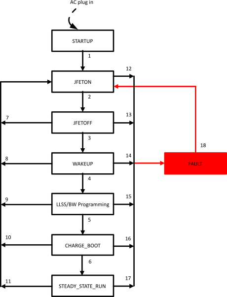
GUID-20220601-SS0I-LGVS-9D5R-VW4P1WBX9GJT-low.png Figure 2-38 State Diagram for UCC25640x
  • Over Temperature (OTP), Low DC Input Voltage (BLK UVLO), Over voltage at the DC Input (BLK OVP), RVCC UVLO will also get part into fault state
  • For “restart” IC version, IC goes into fault state (gate turns off, RVCC shut down, etc) and stays in fault idle state for 1s, before entering JFETON.
  • For “latch” IC version, IC goes into fault state and stay latched. VCC is supplied from HV pin and regulated at ~14.5 V.
  • For external fault protection, pull down the BLK pin voltage.