SLUSDC0C October 2018 – November 2021 UCC21530
PRODUCTION DATA
- 1 Features
- 2 Applications
- 3 Description
- 4 Revision History
- 5 Pin Configuration and Functions
-
6 Specifications
- 6.1 Absolute Maximum Ratings
- 6.2 ESD Ratings
- 6.3 Recommended Operating Conditions
- 6.4 Thermal Information
- 6.5 Power Ratings
- 6.6 Insulation Specifications
- 6.7 Safety-Related Certifications
- 6.8 Safety-Limiting Values
- 6.9 Electrical Characteristics
- 6.10 Switching Characteristics
- 6.11 Insulation Characteristics Curves
- 6.12 Typical Characteristics
- 7 Parameter Measurement Information
- 8 Detailed Description
-
9 Application and Implementation
- 9.1 Application Information
- 9.2
Typical Application
- 9.2.1 Design Requirements
- 9.2.2 Detailed Design Procedure
- 9.2.3 Application Curves
- 10Power Supply Recommendations
- 11Layout
- 12Device and Documentation Support
6.12 Typical Characteristics
VDDA = VDDB = 15 V, VCCI = 3.3 V, TA = 25°C, No load. (unless otherwise noted)
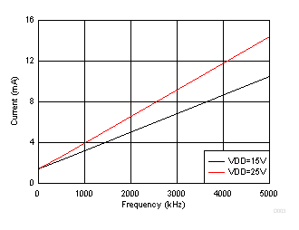
| No load |
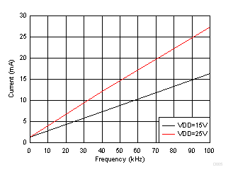
| CLOAD = 10 nF | ||
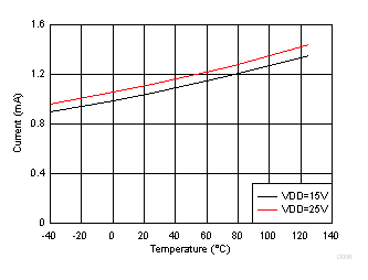
| No load | Input low | No switching |
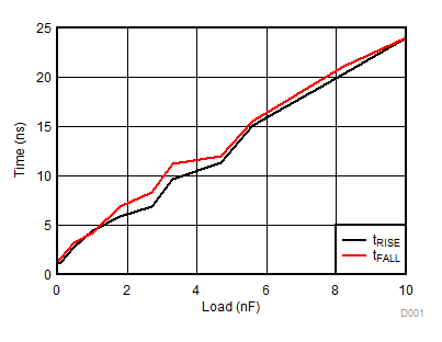 Figure 6-10 Rising and Falling Times vs. Load
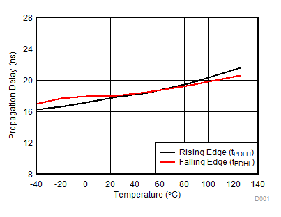 Figure 6-12 Propagation Delay vs. Temperature
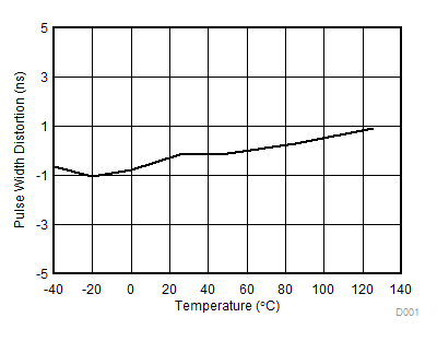 Figure 6-14 Pulse Width Distortion vs. Temperature
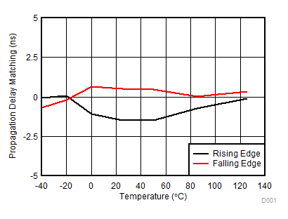 Figure 6-16 Propagation Delay Matching (tDM) vs. Temperature
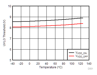 Figure 6-18 8-V UVLO Threshold vs. Temperature
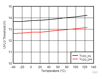 Figure 6-20 12-V UVLO Threshold vs. Temperature
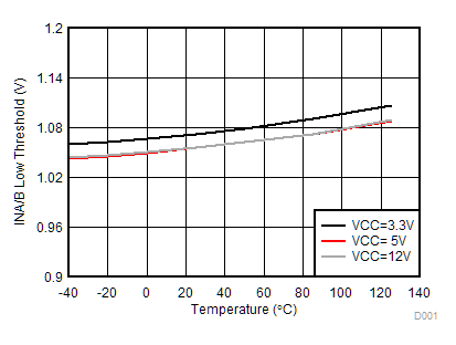 Figure 6-22 INA/B Low Threshold
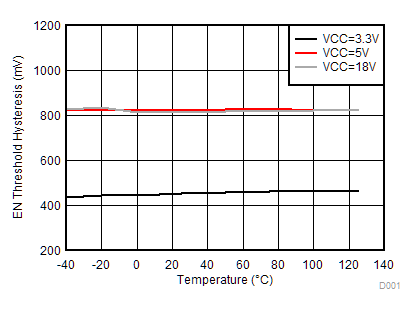 Figure 6-24 EN Threshold Hysteresis vs. Temperature
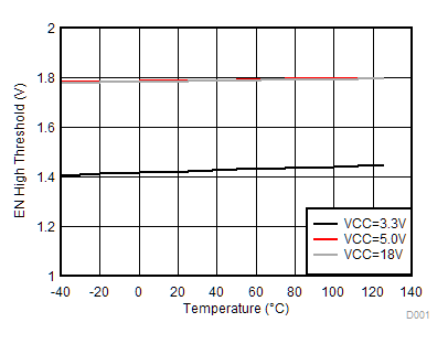 Figure 6-26 EN High Threshold vs.
Temperature
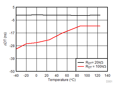 Figure 6-28 Dead Time Matching vs.
Temperature
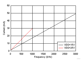
| CLOAD = 1 nF | ||
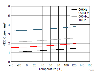
| No load | VDD = 15 V |
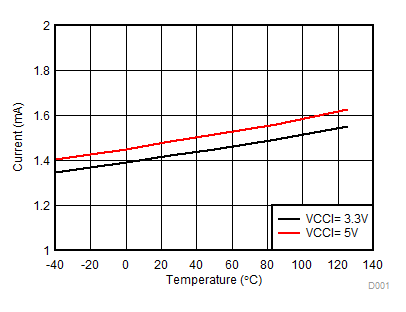
| No load | Input low | No switching |
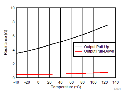 Figure 6-11 Output Resistance vs. Temperature
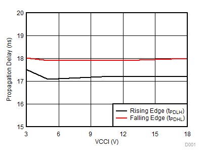 Figure 6-13 Propagation Delay vs. VCCI
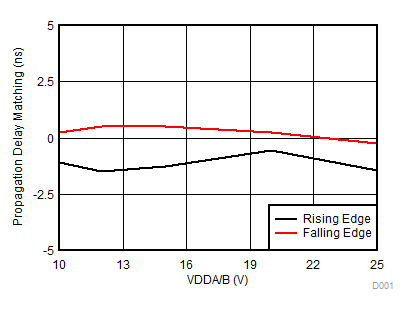 Figure 6-15 Propagation Delay Matching (tDM) vs. VDD
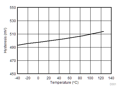 Figure 6-17 8-V UVLO Hysteresis vs. Temperature
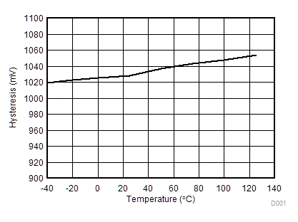 Figure 6-19 12-V UVLO Hysteresis vs. Temperature
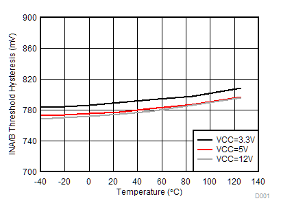 Figure 6-21 INA/B Hysteresis vs. Temperature
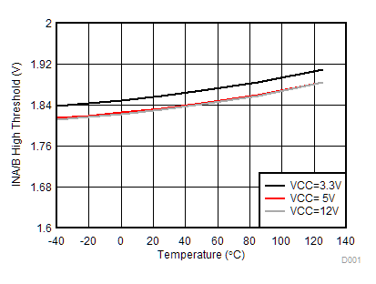 Figure 6-23 INA/B High Threshold
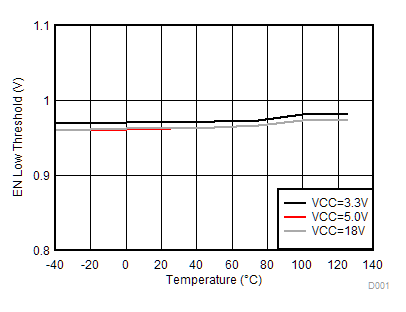 Figure 6-25 EN Low Threshold vs.
Temperature
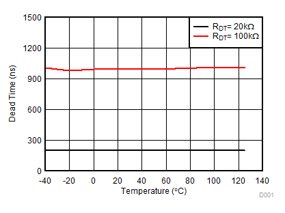 Figure 6-27 Dead Time vs.
Temperature