SLUU182A January   2004  – March 2022 TPS5124


  1.   Trademarks
  2. 1Introduction
  3. 2Features
  4. 3Schematic
  5. 4Design Procedure
    1. 4.1 Frequency Setting
    2. 4.2 Inductance Value
    3. 4.3 Output Capacitors
    4. 4.4 Input Capacitors
      1. 4.4.1 Case One: D1, D2 < 0.5
      2. 4.4.2 Case Two: D2 < 0.5 < D1
    5. 4.5 Compensation Design
    6. 4.6 Current Limiting
    7. 4.7 Timer Latch
      1. 4.7.1 Undervoltage Protection
      2. 4.7.2 Short Circuit Protection
      3. 4.7.3 Overvoltage Protection
      4. 4.7.4 Disabling the Protection Function
        1. 4.7.4.1 Disabling the Overcurrent Protection
        2. 4.7.4.2 Disabling the Overvoltage Protection or Undervoltage Protection
  6. 5Test Results
    1. 5.1 Efficiency Curves
    2. 5.2 Typical Operating Waveform
    3. 5.3 Start-Up Waveform
    4. 5.4 Output Ripple Voltage and Load Transient
  7. 6Layout Guidelines
    1. 6.1 Low-Side MOSFET
    2. 6.2 Connections
    3. 6.3 Bypass Capacitor
    4. 6.4 Bootstrap Capacitor
    5. 6.5 Output Voltage
  8. 7PCB Layout
  9. 8List of Materials
  10. 9Revision History

Output Ripple Voltage and Load Transient

The output ripple is about 20 mVP−P at 15 A on Channel 1 (3.3 V) output and 15 mVP−P at 10 A on Channel 2 output as shown in Figure 5-6.

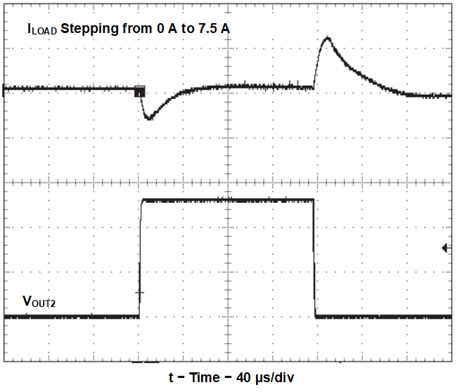
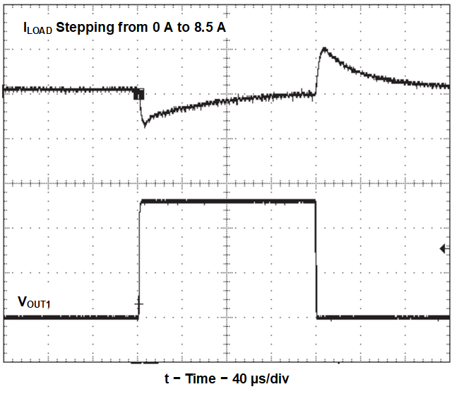
Figure 5-7 shows the load transient response. For Channel 1 (3.3 V), when the load steps from 0 A to 8.5 A, the overshoot and undershoot voltages are about 150 mV. For Channel 2 (1.5 V), when the load steps from 0 A to 7.5 A, the overshoot voltage is approximately 220 mV and the undershoot voltage is approximately 140 mV.
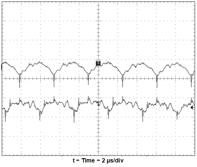
GUID-20220302-SS0I-3QB9-2B8L-W172FZWZS2Z0-low.pngFigure 5-6 Output Ripple
GUID-20220302-SS0I-LTDB-HGKJ-FV61WCSRCBQP-low.pngFigure 5-8 Load Transient Response
GUID-20220302-SS0I-KB7H-5LP0-FN2WSMS31VST-low.pngFigure 5-7 Load Transient Response