SLUUCJ2C july 2021 – august 2023 UCC14240-Q1 , UCC14241-Q1 , UCC15240-Q1 , UCC15241-Q1
5.9.2 Output OVP
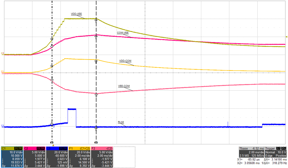
Figure 5-21 shows the effect of mismatched bias loading at startup where the load on VDD-COM is greater than the load on VEE-COM. A fixed resistive load of 910-Ω (247 mW) is applied to VDD-COM while VEE-COM is left unloaded. VDD-VEE is regulating at 20-V, as expected and VDD-COM is measuring 14.5 V (target value is 15 V) but VEE-COM is measuring 5.5 V (target value is 5 V). VEE-COM is directly monitored by FBVEE and has exceeded 110% of the set target value, triggering OVP and instantly latching both outputs off, regardless of the 16-ms watch-dog-timer. When FBVEE has detected the regulated voltage exceeding the set target value, RLIM is internally switched to VEE, sinking current from the capacitor midpoint, COM connection. When activated, as illustrated in Figure 5-21, the outputs are latched off into a protected sate. EN or VIN must be recycled to clear the OVP fault and attempt to restart the module.

| top: VDD-VEE, 10 V/div, | mid3: VEE-COM, 5 V/div, |
| mid1: COM-VEE, 5 V/div, | bot: RLIM, 20 V/div, |
| mid2: VDD-COM, 20 V/div, | time = 2 ms/div |
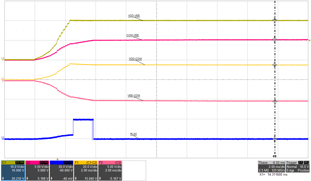
Figure 5-22 shows the same fixed resistive load of 910-Ω (247 mW) applied to VDD-COM as Figure 5-21 but the load on VEE-COM has been increased from 0-mW to 53-mW. Once both outputs are regulating, RLIM is internally connected and held to VEE, sinking current from COM, attempting to compensate for the additional load imbalance present during steady state operation.

| top: VDD-VEE, 10 V/div, | mid3: VEE-COM, 5 V/div, |
| mid1: COM-VEE, 5 V/div, | bot: RLIM, 20 V/div), |
| mid2: VDD-COM, 20 V/div, | time = 2 ms/div |