SLUUCS5A january 2023 – july 2023 UCC14141-Q1
5.9.2 Output OVP
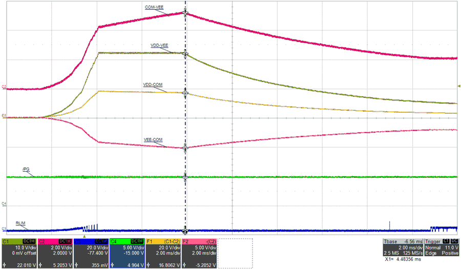
Figure 5-23 shows the effect of mismatched bias loading at startup where the load on VDD-COM is greater than the load on VEE-COM. A fixed resistive load of 1-kΩ (324 mW) is applied to VDD-COM while VEE-COM is left unloaded. VDD-VEE is regulating at 22-V, as expected but VDD-COM is measuring 16.8 V (18-V setpoint) and VEE-COM is measuring 5.2 V (4-V setpoint). COM-VEE is directly monitored by FBVEE and has exceeded 110% of the set target value, triggering OVP and latching both outputs off, regardless of the 28.4-ms watch-dog-timer. When FBVEE has detected the regulated voltage exceeding the set target value, RLIM is internally switched to VEE, sinking current from the capacitor midpoint, COM connection. When activated, as illustrated in Figure 5-23, the outputs are latched off into a protected sate. EN or VIN must be recycled to clear the OVP fault and attempt to restart the module.

Figure 5-23 VEE OVP, VIN=12 V, PVDD=324 mW, PVEE=0 mW, (top: COM-VEE, 2 V/div, mid1: VDD-VEE, 10 V/div, mid2: VDD-COM, 20 V/div, mid3: VEE-COM, 5 V/div, mid4: /PG, 5 V/div, bot: RLIM, 20 V/div), time = 2 ms/div
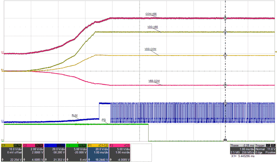
Figure 5-24 shows the same fixed resistive load of 1-kΩ (324 mW) applied to VDD-COM as Figure 5-23but the load on VEE-COM has been increased from 0-mW to 106-mW (150 Ω). VDD and VEE loads are within their respective limits and the RLIM function is shown compensating for the detected load differences.

Figure 5-24 Normal Start, VIN=12 V, PVDD=324 mW, PVEE=106 mW, (top: COM-VEE, 2 V/div, mid1: VDD-VEE, 10 V/div, mid2: VDD-COM, 20 V/div, mid3: VEE-COM, 5 V/div, mid4: RLIM, 20 V/div, bot: /PG, 5 V/div), time = 1 ms/div